Thin film transistor, array substrate, and display device

A technology of thin-film transistors and drain electrodes, which is applied in the direction of transistors, semiconductor devices, electrical components, etc., can solve the problems of poor display effect, achieve the effects of reducing parasitic capacitance, reducing the facing area, and improving performance

Inactive Publication Date: 2019-01-08
SHENZHEN CHINA STAR OPTOELECTRONICS TECH CO LTD
View PDF3 Cites 2 Cited by
  • Summary
  • Abstract
  • Description
  • Claims
  • Application Information

AI Technical Summary

Problems solved by technology

Therefore, after the thin film transistor is turned off, the jump voltage will make the actual pixel voltage less than the charging voltage when the thin film transistor is turned on, resulting in poor display effect

Method used


Image

  • Thin film transistor, array substrate, and display device
  • Thin film transistor, array substrate, and display device
  • Thin film transistor, array substrate, and display device

Examples


Embodiment 1

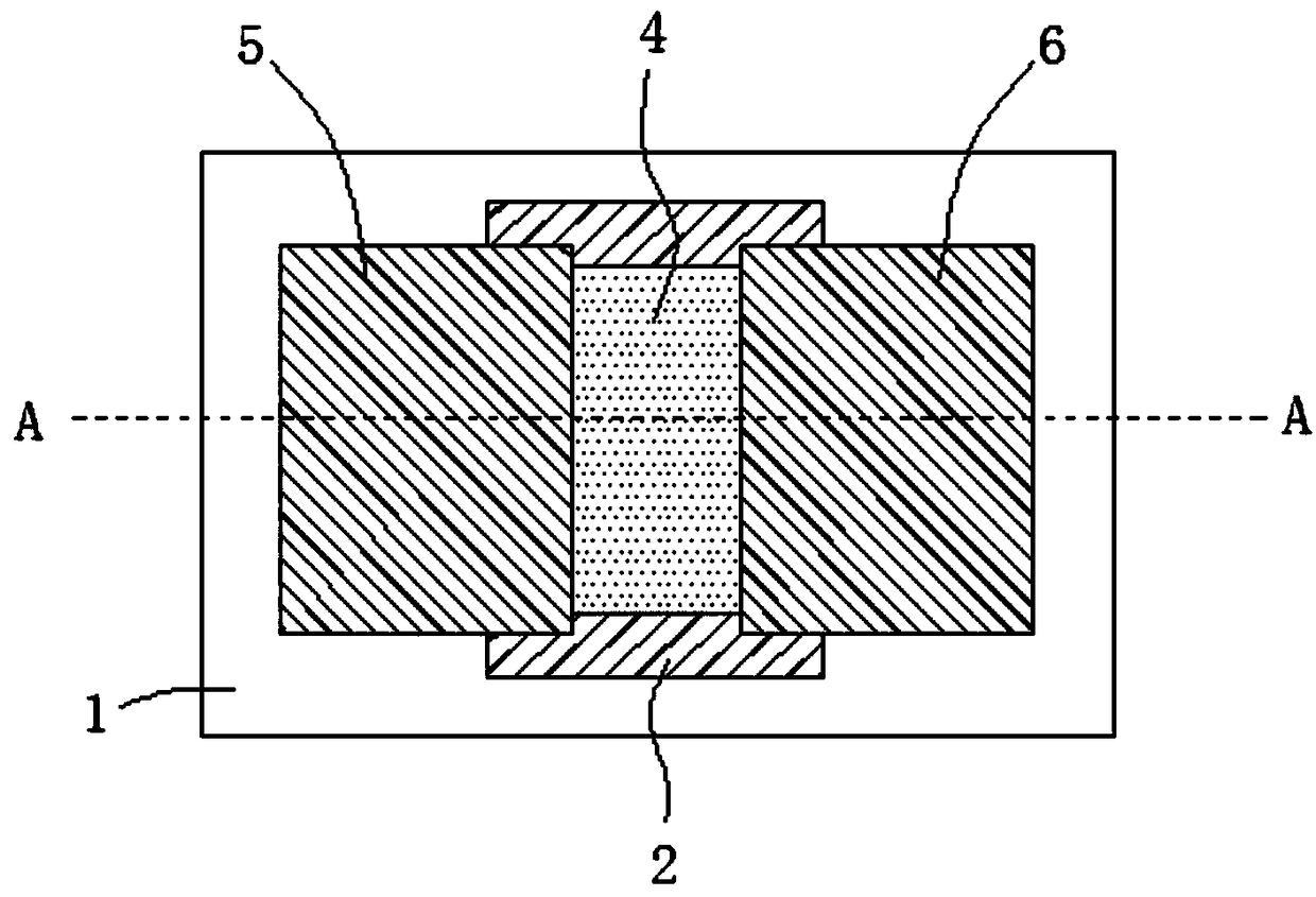
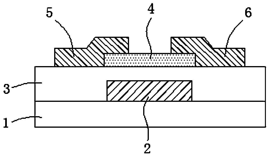
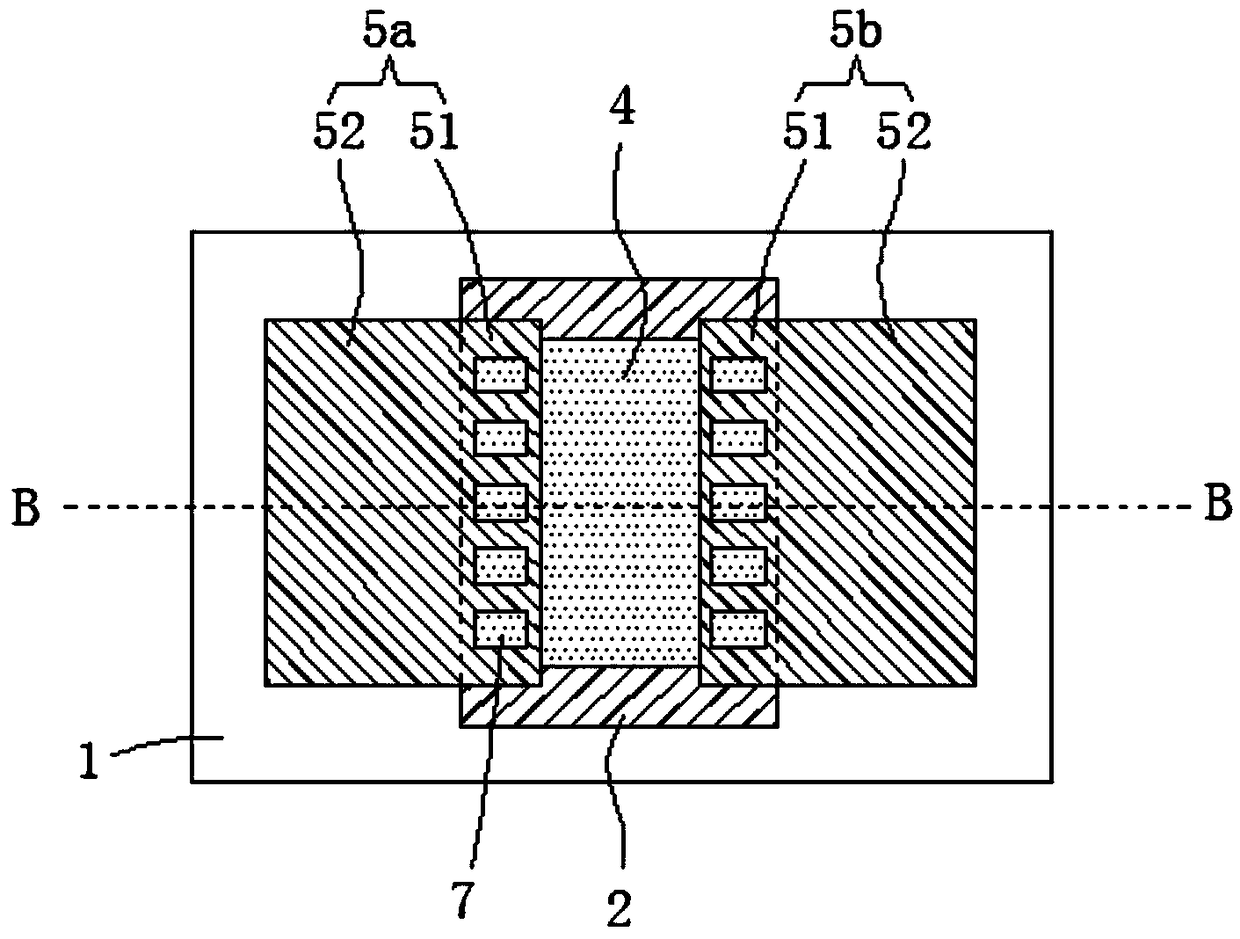
[0033] This embodiment provides a thin film transistor, refer to Figure 3 to Figure 5 , the thin film transistor includes a substrate 1, a gate electrode 2 disposed on the substrate 1, a gate insulating layer 3 covering the gate electrode 2, an active layer 4 disposed on the gate insulating layer 3, and a source electrode 5a and drain electrode 5b. The source electrode 5a and the drain electrode 5b are located in the same structural layer and are spaced apart from each other, the source electrode 5a is connected to the first end of the active layer 4, and the drain electrode 5b is connected to the active layer 4 the second end of .

[0034] Wherein, the source electrode 5 a and the drain electrode 5 b respectively include a first region 51 overlapping with the gate electrode 2 and a second region 52 outside the first region 51 . The first region 51 of the source electrode 5 a and the drain electrode 5 b is formed with a hollow pattern 7 , where the active layer 4 is exposed...

Embodiment 2

[0045] The difference between the thin film transistor provided in this embodiment and Embodiment 1 is that, as Image 6 As shown, in the source electrode 5 a and the drain electrode 5 b, the hollow pattern 7 is formed in the first region 51 and the second region 52 . In the thin film transistor in this embodiment, on the basis of reducing the parasitic capacitance between the gate electrode and the source / drain electrodes, the hollow pattern 7 is also formed in the second region 52, thereby increasing the flexibility of the thin film transistor. The thin film transistor structure provided in this embodiment, when applied to a flexible display device, can improve the bending performance of the flexible display device.

Embodiment 3

[0047] The difference between the thin film transistor provided in this embodiment and Embodiment 1 is that, as Figure 7 and Figure 8 As shown, the first region 51 of the source electrode 5a and the drain electrode 5b is a comb-like structure, the comb-tooth portion 8 of the comb-like structure is connected to the active layer 4, and between two adjacent comb-tooth portions 8 The gap between them is formed as the hollow pattern 7 .

[0048] Specifically, such as Figure 8 As shown, the line width L2 of the comb-tooth portion 8 is preferably set to 1-5 μm, and the distance D2 between two adjacent comb-tooth portions 8 (ie the width of the hollow pattern 7 ) is preferably set to 1-10 μm.

[0049] It should be noted that, as a structural change of this embodiment, the manner of Embodiment 2 can be referred to, and the second region 52 of the source electrode 5a and the drain electrode 5b in this embodiment is also provided with a hollow pattern 7 to improve Flexible properti...


PUM


Abstract

A thin film transistor is disclosed. A gate electrode, gate insulating layer, an active layer and source and drain electrodes are sequentially formed on a substrate, the source electrode is connectedto a first end of the active layer, the drain electrode is connected to a second end of the active layer, The source electrode and the drain electrode respectively include a first region overlapping with the gate electrode and a second region located outside the first region, wherein at least the first region of the source electrode and the drain electrode is formed with a hollow pattern to reducean area directly opposite the source electrode and the drain electrode to the gate electrode. An array substrate and a display device including a thin film transistor as described above are also disclosed. The thin film transistor provided above can reduce the area of the source/drain electrode facing the gate electrode, reduce the parasitic capacitance, and improve the performance of the device.

Description

technical field [0001] The present invention relates to the technical field of displays, in particular to a thin film transistor, an array substrate containing the thin film transistor, and a display device. Background technique [0002] The flat panel display device has many advantages such as thin body, power saving, and no radiation, and has been widely used. Existing flat panel display devices mainly include liquid crystal display devices (Liquid Crystal Display, LCD) and organic electroluminescent display devices (Organic Light Emitting Display, OLED). A thin film transistor (Thin Film Transistor, TFT) is an important part of a flat panel display device, which can be formed on a glass substrate or a plastic substrate, and is usually used as a switching device and a driving device such as LCD and OLED. [0003] figure 1 is a schematic top view of an existing thin film transistor, figure 2 For such figure 1 The schematic cross-sectional view of the thin film transist...

Claims


Application Information

Patent Timeline
Patent Type & Authority Applications(China)
IPC IPC(8): H01L29/417H01L29/423H01L29/786
CPCH01L29/41733H01L29/42384H01L29/78654H01L29/7869
Inventor 罗传宝
Owner SHENZHEN CHINA STAR OPTOELECTRONICS TECH CO LTD
Why Eureka
Try Eureka