Organic light emitting diode touch panel and method of forming same

A technology of light-emitting diodes and touch panels, which is applied to instruments, computing, and electrical digital data processing. The effect of precision

Active Publication Date: 2019-12-17
WUHAN CHINA STAR OPTOELECTRONICS SEMICON DISPLAY TECH CO LTD
View PDF8 Cites 0 Cited by
  • Summary
  • Abstract
  • Description
  • Claims
  • Application Information

AI Technical Summary

Problems solved by technology

Where the second conductive layer crosses the first conductive layer, a bridging method is adopted. However, due to the small area of ​​the bridging connection, the contact resistance at this place is relatively large, and the power consumption increases.

Method used


Image

  • Organic light emitting diode touch panel and method of forming same
  • Organic light emitting diode touch panel and method of forming same
  • Organic light emitting diode touch panel and method of forming same

Examples


Embodiment Construction

[0025] The following descriptions of the various embodiments refer to the accompanying drawings to illustrate specific embodiments in which the present invention can be practiced. The directional terms mentioned in the present invention, such as "up", "down", "front", "back", "left", "right", "top", "bottom", "horizontal", "vertical" etc. , are for orientation only with reference to the attached drawings. Therefore, the directional terms used are used to illustrate and understand the present invention, but not to limit the present invention.

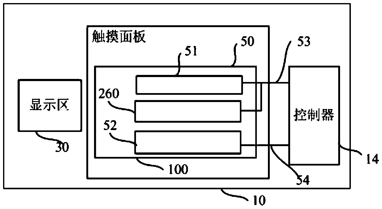
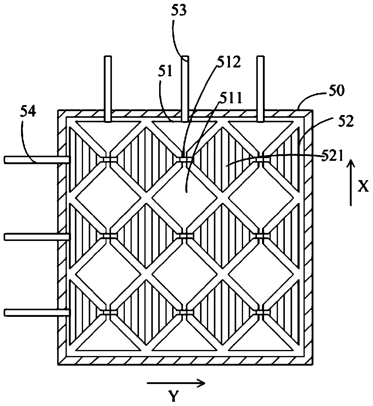
[0026] see figure 1 as well as figure 2 , figure 1 is a schematic diagram of a display device 10 according to an embodiment of the present invention, figure 2 It is a partial structure diagram of the touch area 50 of the touch panel of this embodiment. The display device 10 includes a display area 30 , a touch panel 100 and a controller 14 . The touch panel 100 is an organic light emitting diode (OLED) display panel with a touch ...


PUM


Abstract

An organic light-emitting diode touch panel comprises an organic light-emitting diode structure, a first conductive layer, a second conductive layer, a sense conductive layer, a third conductive layer and multiple second sense electrodes. The second conductive layer comprises multiple first sense electrodes. The sense conductive layer is positioned above the sense conductive layer and is in contact with the multiple first sense electrodes. The third conductive layer comprises multiple second drive electrodes. The first conductive layer is electrically connected to the third conductive layer.

Description

【Technical field】 [0001] The invention relates to the technical field of capacitive sensing, in particular to a mutual capacitive organic light emitting diode touch panel and a forming method thereof. 【Background technique】 [0002] Organic Light-Emitting Diode (OLED) touch panels are gradually and widely used in mobile terminals due to their flexibility, bright colors and high touch accuracy. Touch technology is divided into on-cell and in-cell technologies. The on-cell technology is to directly manufacture the touch electrodes on the thin film encapsulation layer of the OLED. However, the on-cell technology that directly manufactures capacitive sensing components on the OLED panel will be affected by the cathode of the OLED, which will cause interference to the driving signal and make the change in sensing capacitance before and after touch is small, making it difficult to monitor the touch chip. On the other hand, the current capacitive sensing components include a plur...

Claims


Application Information

Patent Timeline
Patent Type & Authority Patents(China)
IPC IPC(8): G06F3/041G06F3/044
CPCG06F3/0412G06F3/044G06F2203/04103
Inventor 周宏玉
Owner WUHAN CHINA STAR OPTOELECTRONICS SEMICON DISPLAY TECH CO LTD
Why Eureka
Try Eureka