Home environment quality monitoring device based on STM32 single chip microcomputer
A technology of environmental quality and monitoring devices, applied to measuring devices, instruments, etc., can solve problems such as waste, less functions of detectors, and inability to network, and achieve the effects of low cost, cost reduction, and simple operation
- Summary
- Abstract
- Description
- Claims
- Application Information
AI Technical Summary
Problems solved by technology
Method used
Image
Examples
Embodiment 1
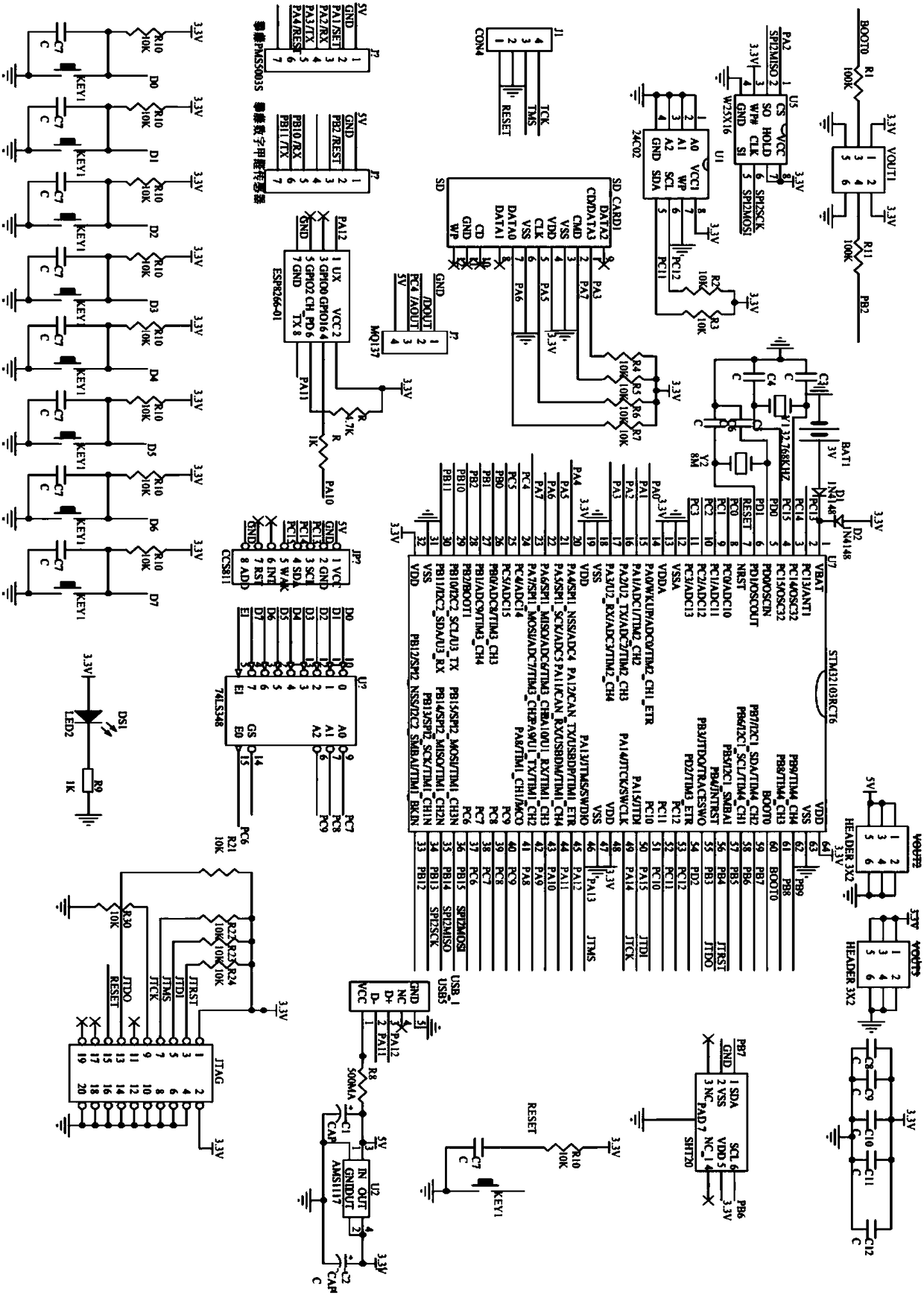
[0025] Such as figure 1 As shown, the home environment quality monitoring device based on the STM32 single-chip microcomputer of the present embodiment includes a STM32F103 single-chip microcomputer, an environmental quality measurement module, a sensor identification circuit and a Wi-Fi module; connection, the STM32F103 microcontroller is connected to the Wi-Fi module through an IO port. The input end of described sensor identification circuit is provided with the interface that is connected for described each environmental quality measuring module, and the output end of described sensor identification circuit is connected with described STM32F103 single-chip microcomputer by IO port. A button is placed next to the interface of each environmental quality measurement module. After the selected environmental quality measurement module is connected, press the button, and the STM32F103 single-chip microcomputer judges which measurement modules have been connected through the valu...
Embodiment 2
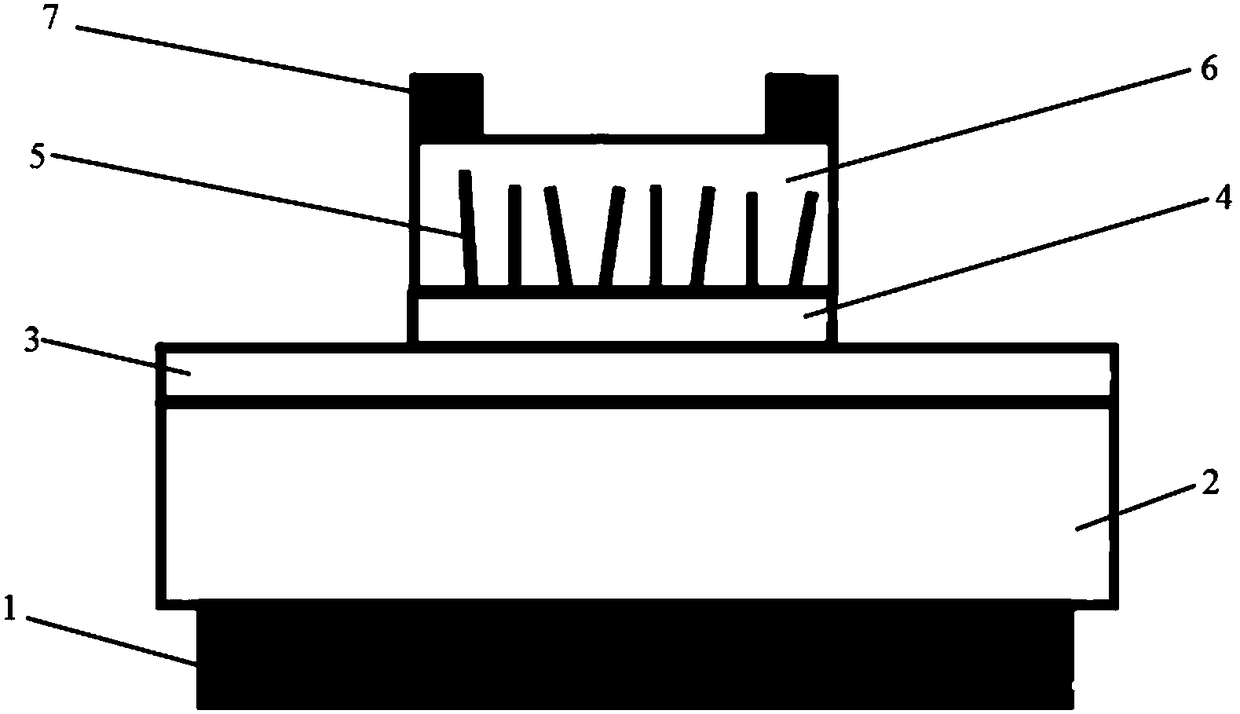
[0034] The difference between this embodiment and the first embodiment is that the home environment quality monitoring device based on the STM32 single-chip microcomputer of this embodiment also includes a carbon monoxide gas sensor, and the carbon monoxide gas sensor is connected to the STM32F103 single-chip microcomputer through the IO port after AD conversion. The carbon monoxide gas sensor includes a heating module 1, a Si substrate 2 arranged above the heating module, a silicon oxide film 3 formed on the Si substrate, a W film 4 arranged on the silicon oxide film, and a silicon oxide film 4 formed on the silicon oxide film. WO3 nanowire film 5 on the W film, SnO2 nanofilm 6 covering the WO3 nanowire film 5, and two Pt electrodes 7 arranged on the SnO2 nanofilm.
[0035] The thickness of the silicon oxide thin film 3 is 400-500 nm, the thickness of the W film 4 is 200-250 nm, and the length of the WO3 nanowire is 1000-1500 nm.
PUM
 Abstract
Description
Claims
Application Information


