

A method for additively manufacturing copper circuit board patterns
A technology of additive manufacturing and circuit boards, which is applied in printed circuit manufacturing, conductive pattern formation, printed circuit, etc., can solve the problem of high thermal conductivity, low heat absorption rate, low laser energy utilization rate, and difficulty in melting copper alloy powder layer by layer And other problems, to achieve broad application prospects, to meet the rapid effect
- Summary
- Abstract
- Description
- Claims
- Application Information
AI Technical Summary
Problems solved by technology
Method used
Image

Examples
Embodiment 1
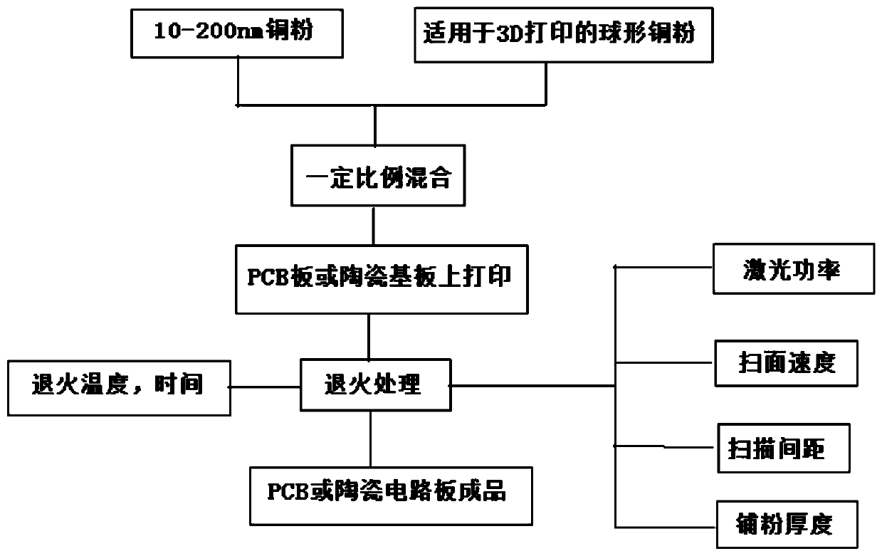
[0017] Utilize the present invention to prepare a kind of concrete method step of copper circuit board pattern as follows:
[0018] (1) Select nano-copper powder with a particle size ranging from 10 to 50 nm;
[0019] (2) Mix the nano-powder selected in step (1) with the spherical powder whose particle size range is 30-50 μm according to the ratio of 1:3;
[0020] (3) Use the mixed powder in step (2) to print the predetermined circuit pattern on the PCB by controlling the laser power of 50W, the scanning rate of 200mm / s, the scanning distance of 0.01mm, and the powder thickness of 0.05mm by using a 3D printer;
[0021] (4) The printed PCB circuit board in step (3) is annealed and stress-relieved at a temperature of 220° C. in a reduction furnace for 3 hours.
Embodiment 2
[0023] Utilize the present invention to prepare a kind of concrete method step of copper circuit board pattern as follows:
[0024] (1) Select nano-copper powder with a particle size ranging from 50 to 100 nm;
[0025] (2) Mix the nano-powder selected in step (1) with the spherical powder whose particle size range is 50-75 μm according to the ratio of 1:3;
[0026] (3) Use the mixed powder in step (2) to print the predetermined circuit pattern on the PCB by controlling the laser power of 75W, the scanning rate of 350mm / s, the scanning distance of 0.03mm, and the powder thickness of 0.075mm by using a 3D printer;
[0027] (4) The printed PCB circuit board in step (3) is annealed and stress-relieved at a temperature of 260° C. in a reduction furnace for 2 hours.
Embodiment 3
[0029] Utilize the present invention to prepare a kind of concrete method step of copper circuit board pattern as follows:
[0030] (1) Select nano-copper powder with a particle size ranging from 100 to 200 nm;
[0031] (2) Mix the nano-powder selected in step (1) with the spherical powder with a particle size range of 75-100 μm in a ratio of 1:3;
[0032] (3) Use the mixed powder in step (2) to print the predetermined circuit pattern on the ceramic substrate by controlling the laser power of 100W, the scanning rate of 500mm / s, the scanning distance of 0.05mm, and the powder thickness of 0.1mm by using a 3D printer ;
[0033] (4) The ceramic circuit board printed in step (3) is annealed and stress-relieved at a temperature of 300° C. in a reduction furnace for 1 hour.
PUM
| Property | Measurement | Unit |
|---|---|---|
| thickness | aaaaa | aaaaa |
| melting point | aaaaa | aaaaa |
| melting point | aaaaa | aaaaa |
Abstract
Description
Claims
Application Information