Array substrate and liquid crystal display panel

An array substrate, liquid crystal technology, applied in instruments, nonlinear optics, optics, etc., can solve problems such as affecting light transmittance

Active Publication Date: 2021-07-06
CHENGDU ZHONGDIAN PANDA DISPLAY TECH CO LTD
View PDF7 Cites 0 Cited by
  • Summary
  • Abstract
  • Description
  • Claims
  • Application Information

AI Technical Summary

Problems solved by technology

[0004] However, using this UV 2 In the liquid crystal panel aligned by technology A, the pixel structure will be formed at the junction between the four alignment sub-regions of each sub-pixel, that is, in the middle of the sub-pixel. figure 2 The roughly cross-shaped dark lines 40 shown affect the light transmittance

Method used


Image

  • Array substrate and liquid crystal display panel
  • Array substrate and liquid crystal display panel
  • Array substrate and liquid crystal display panel

Examples


Embodiment 1

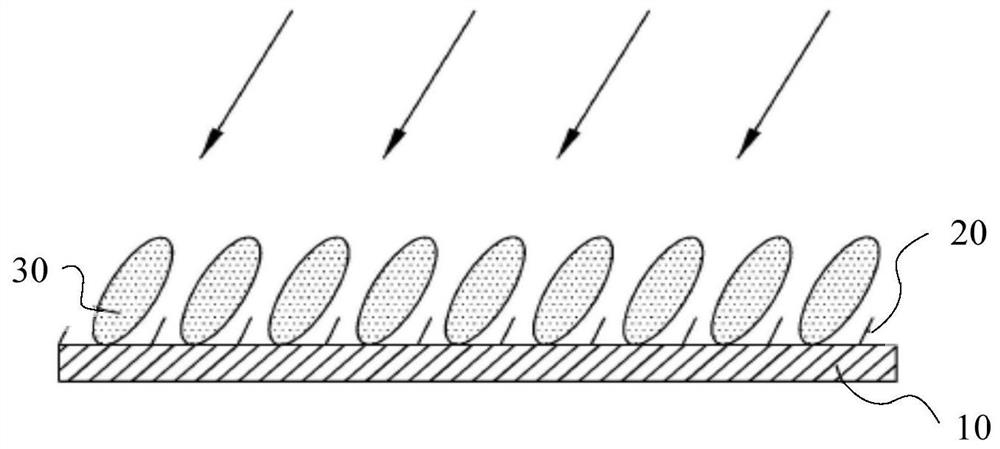
[0044] image 3 It is a schematic plan view of the part corresponding to the first region in the array substrate provided by Embodiment 1 of the present invention. Figure 4 A cross-sectional view of a part corresponding to the first region in the array substrate provided by Embodiment 1 of the present invention. In order to illustrate how to reduce the generation of dark lines, image 3 , Figure 4 Only the schematic diagram of the part corresponding to the two first regions 6 (sub-pixel units) in the array substrate is shown.

[0045] Such as image 3 , 4 As shown, the array substrate 1 of this embodiment includes an insulating layer 2 and an indium tin oxide semiconductor layer 3 disposed on the insulating layer 2, the upper side of the indium tin oxide semiconductor layer 3 is in contact with the liquid crystal 4, and the array substrate 1 further includes A plurality of sub-pixel units 5 located under the insulating layer 2, the indium tin oxide semiconductor layer 3...

Embodiment 2

[0053] On the basis of the first embodiment, this embodiment improves the arrangement of the first groove in the first embodiment above. Other parts are the same as those in Embodiment 1, and will not be repeated here.

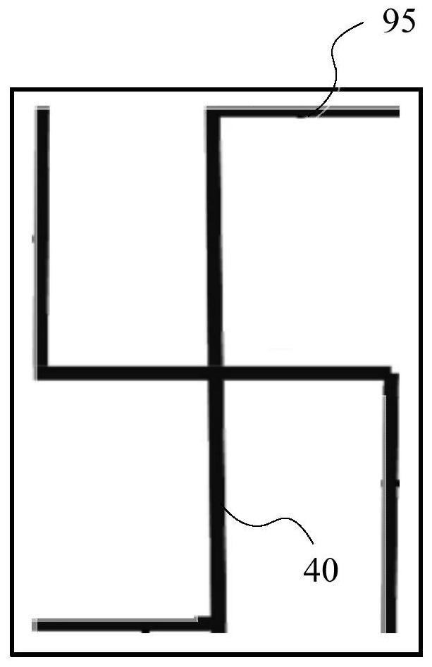
[0054] Figure 6 A cross-sectional view of a part corresponding to the first region in the array substrate provided by Embodiment 2 of the present invention. Such as Figure 6 As shown, the first groove 9 runs through the ITO semiconductor layer 3 . This method is applied to the situation where the thickness of the indium tin oxide semiconductor layer 3 is relatively thin. At this time, in order to ensure sufficient edge effects on the liquid crystal molecules, it is necessary to form the corresponding part of the indium tin oxide semiconductor layer 3 and the first groove 9 It is a hollow cross.

[0055] In addition, compared with the case where the first groove 9 does not penetrate the indium tin oxide semiconductor layer 3, it needs to etch the surface ...

Embodiment 3

[0058] On the basis of the second embodiment, this embodiment further improves the groove portion in the second embodiment. The remaining parts are the same as those in Embodiment 2, and will not be repeated here.

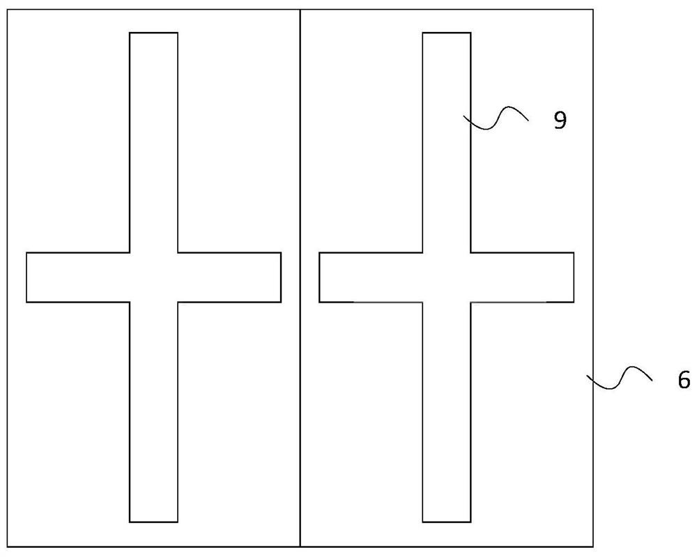
[0059] Figure 7 A cross-sectional view of a part corresponding to the first region in the array substrate provided by Embodiment 3 of the present invention. Such as Figure 7 As shown, on the basis that the first groove 9 in the second embodiment penetrates the indium tin oxide semiconductor layer 3, a plurality of second grooves are formed on the surface of the insulating layer 2 that is in contact with the indium tin oxide semiconductor layer 3. Groove 92 , the projection of the plurality of second grooves 92 on the normal direction of the array substrate 1 coincides with the plurality of first grooves 9 . This method is applied to the situation where the thickness of the indium tin oxide semiconductor layer 3 is relatively thin. At this time, in order to ens...


PUM

PropertyMeasurementUnit
widthaaaaaaaaaa
depthaaaaaaaaaa

Abstract

The invention provides an array substrate and a liquid crystal display panel, comprising an insulating layer and an indium tin oxide semiconductor layer arranged on the insulating layer, the upper side of the indium tin oxide semiconductor layer is in contact with the liquid crystal, and the array substrate further includes a plurality of For the sub-pixel unit below, the indium tin oxide semiconductor layer includes a plurality of first regions whose number is the same as that of the sub-pixel unit, wherein the size of the first region is the same as that of the sub-pixel unit, and the first region is the same as the number of the sub-pixel unit. The units are arranged in one-to-one correspondence, and a first groove is provided in the middle of at least one first region, and the first groove is cross-shaped. The invention can reduce the dark lines in each sub-pixel and improve the light transmittance.

Description

technical field [0001] The invention relates to the technical field of liquid crystal display, in particular to an array substrate and a liquid crystal display panel. Background technique [0002] Liquid Crystal Display (LCD) has many advantages such as thin body, power saving, and no radiation, and has been widely used, such as LCD TV, mobile phone, personal digital assistant, digital camera, computer screen or notebook computer screen, etc. . As far as TFT-LCD liquid crystal panels on the mainstream market are concerned, they can be divided into three categories, namely twisted nematic / super twisted nematic (TN / STN) type, in-plane switching (IPS) type and vertical alignment (VA) type. type. In the manufacturing process of the liquid crystal display panel, the alignment of the guide film is an important process, and the liquid crystal molecules are arranged according to a specific direction and angle through the alignment process. The traditional alignment process adopts...

Claims


Application Information

Patent Timeline
Patent Type & Authority Patents(China)
IPC IPC(8): G02F1/1337
CPCG02F1/133707G02F1/133753G02F1/133788
Inventor 杨仁光
Owner CHENGDU ZHONGDIAN PANDA DISPLAY TECH CO LTD
Why Eureka
Try Eureka