CMOS-TDI image sensor and forming method thereof

An image sensor and pixel area technology, applied in the semiconductor field, can solve problems such as poor performance and increased noise in the voltage domain, and achieve the effect of less loss and improved transmission efficiency

Active Publication Date: 2019-01-25
BRIGATES MICROELECTRONICS KUNSHAN
View PDF4 Cites 4 Cited by
  • Summary
  • Abstract
  • Description
  • Claims
  • Application Information

AI Technical Summary

Problems solved by technology

The output voltage signals of all M rows are accumulated. For an M-class TDI image sensor, the signal is increased by M times, but

Method used


Image

  • CMOS-TDI image sensor and forming method thereof
  • CMOS-TDI image sensor and forming method thereof
  • CMOS-TDI image sensor and forming method thereof

Examples


Embodiment Construction

[0026] As mentioned in the background, the performance of CMOS-TDI image sensors is still poor.

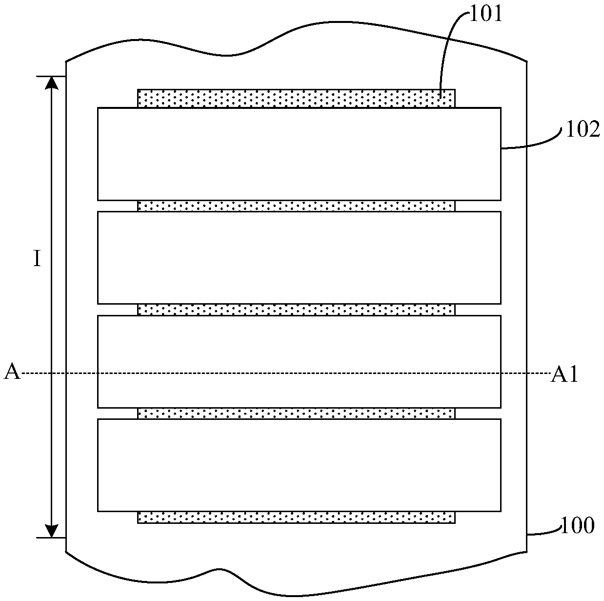
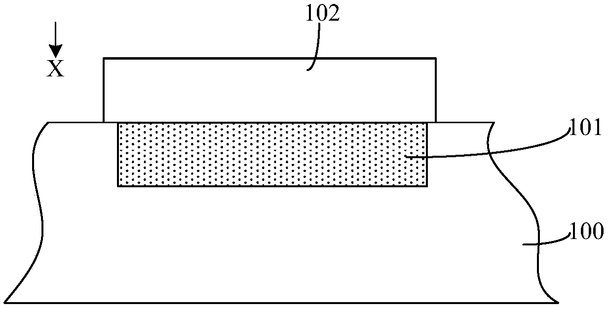
[0027] figure 1 and figure 2 It is a schematic diagram of the structure of a CMOS-TDI image sensor.

[0028] Please refer to figure 1 and figure 2 , figure 2 yes figure 1 Schematic diagram of the cross-sectional structure along the line A-A1, figure 1 yes figure 2 In the top view along the X direction, a substrate 100 is provided, the substrate 100 includes several pixel regions I, and a first doped region 101 is formed in the pixel region I; a gate is formed on the surface of the substrate 100 in the pixel region I structure 102 , the gate structure 102 straddles the first doped region 101 .

[0029] In the above CMOS-TDI image sensor, the method for forming the first doped region 101 includes: forming a mask layer (not shown in the figure) on part of the surface of the substrate 100, and the mask layer exposes the pixel region I The surface of the substrate 100 ; us...


PUM

PropertyMeasurementUnit
Sizeaaaaaaaaaa
Depthaaaaaaaaaa

Abstract

provided are a CMOS-TDI image sensor and forming method thereof, wherein the CMOS-TDI image sensor includes a substrate including a plurality of pixel region; A plurality of mutually discrete first doped regions located within a substrate of each of the pixel regions; A first gate structure located on a substrate surface of each pixel region, the first gate structure spanning a plurality of firstdoped regions. The advantage of that CMOS-TDI image sensor can improve charge transfer efficiency and image quality.

Description

technical field [0001] The invention relates to the field of semiconductors, in particular to a CMOS-TDI image sensor and a forming method thereof. Background technique [0002] A Time Delay Integration (TDI) image sensor is an evolution of a linear image sensor. The imaging mechanism of the time-delay integral image sensor is to expose the pixels passed by the object one by one, and accumulate the exposure structure, so as to solve the problem of weak imaging signal caused by insufficient exposure time of high-speed moving objects. The time-delay integral image sensor can increase the effective exposure time and improve the image signal-to-noise ratio. [0003] There are two types of time-delay integration image sensors, CCD and CMOS. However, due to the particularity of the CCD process, other processing circuits cannot be integrated on the image sensor, and the versatility and flexibility are poor. [0004] Another type of TDI image sensor is a CMOS type. This TDI image ...

Claims


Application Information

Patent Timeline
IPC IPC(8): H01L27/146
CPCH01L27/14607H01L27/1461H01L27/14643H01L27/14689
Inventor 王林黄金德
Owner BRIGATES MICROELECTRONICS KUNSHAN
Why Eureka
Try Eureka