Thin film deposition method and josephson junction preparation method
A thin film deposition, superconducting thin film technology, applied in the manufacture/processing of superconducting devices, superconducting devices, electrical components, etc., can solve the problem of low film performance, Josephson junction leakage current, and difficulty in obtaining roughness of superconducting thin films at the same time and stress and other issues to achieve the effect of improving performance, improving performance and stability, and avoiding leakage current.
- Summary
- Abstract
- Description
- Claims
- Application Information
AI Technical Summary
Problems solved by technology
Method used
Image

Examples
Embodiment 1
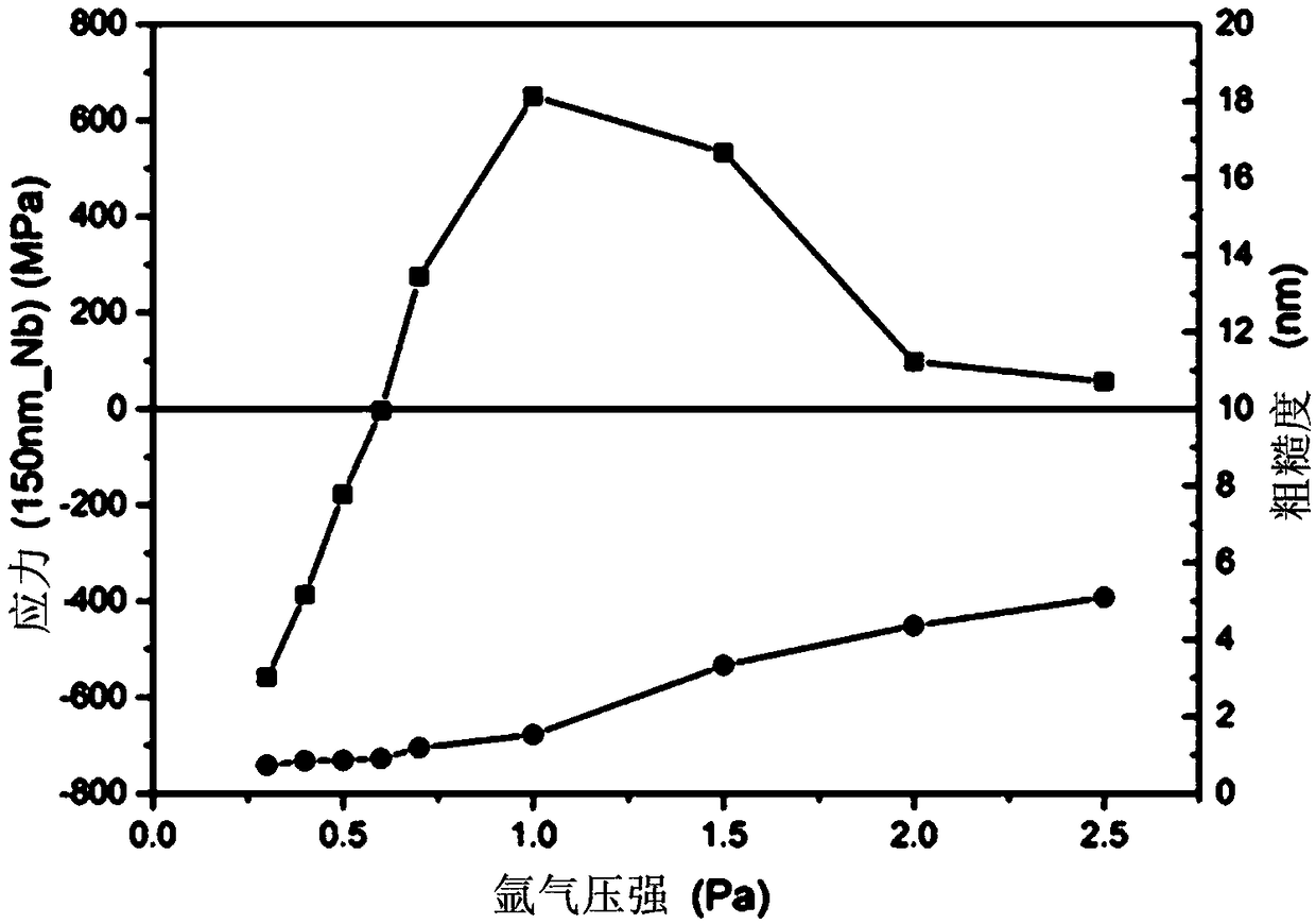
[0040] Before adopting the thin film deposition method of the present invention for thin film deposition, a very important preliminary work is to characterize the stress and roughness of single-layer thin film deposition, and obtain the curve diagram of stress and roughness changing with deposition conditions, such as figure 1 As shown, the schematic diagram of the stress and roughness of the niobium film changing with the deposition conditions is the inventor's long-term research work, after a long period of analysis, repeated experiments and constant adjustment of deposition parameters and finally obtained, according to This curve is a schematic diagram. In the process of actually preparing a superconducting thin film, suitable deposition conditions can be selected according to the performance parameters of the superconducting thin film to be prepared. In this embodiment, an exemplary description will be given to the deposition method of the niobium film according to the sche...
Embodiment 2
[0059] The present invention also provides a method for preparing a Josephson junction, comprising the steps of:
[0060] 1) providing a substrate;
[0061] 2) depositing a superconducting thin film layer on the surface of the substrate;
[0062] 3) depositing an insulating layer on the lower superconducting thin film layer;
[0063] 4) depositing a superconducting thin film layer on the insulating layer;
[0064] Wherein, at least one of the lower superconducting thin film layer and the upper superconducting thin film layer is formed by the thin film deposition method as described in Embodiment 1, that is, the lower superconducting thin film layer and the upper superconducting thin film layer At least one of the two conductive thin film layers is deposited by the stepwise deposition method shown in Embodiment 1, and preferably both are formed by the thin film deposition method in Embodiment 1. By depositing the same film several times, a film that meets the requirements in...
PUM
| Property | Measurement | Unit |
|---|---|---|
| Thickness | aaaaa | aaaaa |
Abstract
Description
Claims
Application Information
 - R&D Engineer
- R&D Manager
- IP Professional
- Industry Leading Data Capabilities
- Powerful AI technology
- Patent DNA Extraction
Browse by: Latest US Patents, China's latest patents, Technical Efficacy Thesaurus, Application Domain, Technology Topic.
© 2024 PatSnap. All rights reserved.Legal|Privacy policy|Modern Slavery Act Transparency Statement|Sitemap