

A diamond-based multi-channel barrier control field effect transistor and its preparation method
A diamond and field regulation technology, which is applied in transistors, semiconductor/solid-state device manufacturing, semiconductor devices, etc., can solve problems such as reducing surface channel carrier concentration and mobility, sacrificing the maximum current of source and drain, and external transconductance. To achieve the effect of ensuring current transport capacity and strong carrier depletion capacity
- Summary
- Abstract
- Description
- Claims
- Application Information
AI Technical Summary
Problems solved by technology
Method used
Image

Examples
Embodiment 1
[0062] A method for preparing a diamond-based multi-channel barrier control field effect transistor, comprising the following steps:
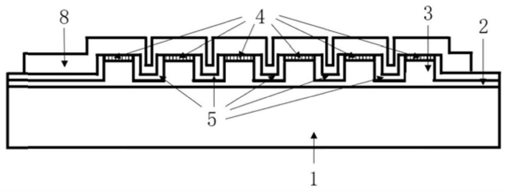
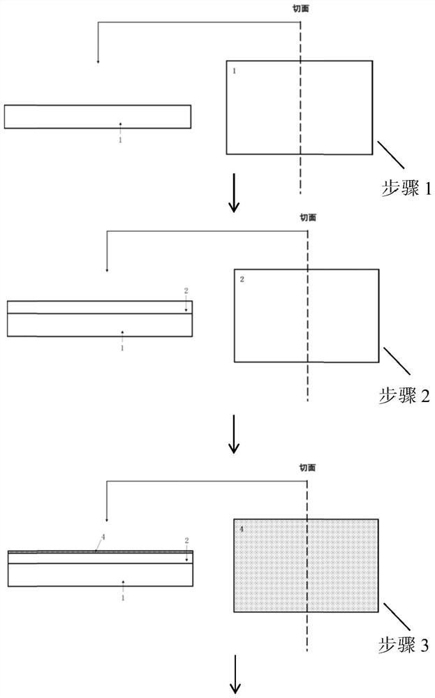
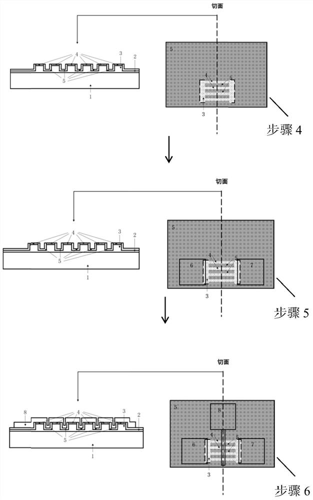
[0063] 1) The diamond substrate 1 grown by high temperature and high pressure (HPHT) technology is cleaned successively by using the standard cleaning process for diamond substrates, followed by inorganic and organic cleaning, and blown dry with nitrogen gas for later use.
[0064] 2) Deposit a single crystal diamond film 2 on the cleaned diamond substrate using microwave plasma vapor chemical deposition (MPCVD), the plasma power is 1kW, the chamber pressure is 100Torr, and the total gas flow is 500sccm, and the obtained single crystal diamond The thickness of the film is 1μm, the resistivity is greater than 100MΩ·cm, the root mean square surface roughness is less than 0.5nm, and the half-peak width of the Raman curve is less than 2cm -1 , XRD rocking curve half width less than 30arcsec.
Embodiment 2
[0070] A method for preparing a diamond-based multi-channel barrier control field-effect transistor comprises the following steps:
[0071] 1) The diamond substrate 1 grown by CVD technology is successively cleaned inorganically and organically by using a standard cleaning process for diamond substrates, and blown dry with nitrogen gas for later use.
[0072] 2) Deposit a single crystal diamond film 2 on the cleaned diamond substrate using microwave plasma vapor chemical deposition (MPCVD), the plasma power is 1kW, the chamber pressure is 100Torr, and the total gas flow is 500sccm, and the obtained single crystal diamond The thickness of the film is 1μm, the resistivity is greater than 100MΩ·cm, the root mean square surface roughness is less than 0.5nm, and the half-peak width of the Raman curve is less than 2cm -1 , XRD rocking curve half width less than 30arcsec.
[0073] 3) Control the power of the microwave plasma so that the chamber temperature is 700° C., keep the hydro...
Embodiment 3
[0078] A method for preparing a diamond-based multi-channel barrier control field-effect transistor comprises the following steps:
[0079] 1) The diamond substrate 1 grown by CVD technology is successively cleaned inorganically and organically by using a standard cleaning process for diamond substrates, and blown dry with nitrogen gas for later use.
[0080] 2) Deposit a single crystal diamond film 2 on the cleaned diamond substrate using microwave plasma vapor chemical deposition (MPCVD), the plasma power is 1kW, the chamber pressure is 100Torr, and the total gas flow is 500sccm, and the obtained single crystal diamond The thickness of the film is 1μm, the resistivity is greater than 100MΩ·cm, the root mean square surface roughness is less than 0.5nm, and the half-peak width of the Raman curve is less than 2cm -1 , XRD rocking curve half width less than 30arcsec.
[0081] 3) Control the microwave plasma power so that the chamber temperature is 900° C., keep the hydrogen gas...
PUM
| Property | Measurement | Unit |
|---|---|---|
| electrical resistivity | aaaaa | aaaaa |
| surface roughness | aaaaa | aaaaa |
| width | aaaaa | aaaaa |
Abstract
Description
Claims
Application Information