A body-doped diamond-based normally-off field-effect transistor and its preparation method

A field effect transistor, diamond technology

Active Publication Date: 2020-08-18
XI AN JIAOTONG UNIV
View PDF6 Cites 0 Cited by
  • Summary
  • Abstract
  • Description
  • Claims
  • Application Information

AI Technical Summary

Problems solved by technology

The body-doped diamond-based normally-off field effect transistor of the present invention utilizes the high Schottky barrier produced by the sidewall of the etching region and the gate metal and the Schottky barrier produced by the surface of the channel region and the gate metal. The effect completely depletes the carriers under the gate (in the channel), causing the conductive channel to be pinched off, so that the device shows normally-off characteristics; the two-dimensional hole gas of the hydrogen-terminated diamond is replaced by bulk-doped diamond as the conductive channel It can solve the problem of the degradation or even disappearance of the electrical properties of the two-dimensional hole gas channel under high temperature or oxygen environment, and can also improve the electrical characteristics of the transistor, such as breakdown field strength and current density.

Method used


Image

  • A body-doped diamond-based normally-off field-effect transistor and its preparation method
  • A body-doped diamond-based normally-off field-effect transistor and its preparation method
  • A body-doped diamond-based normally-off field-effect transistor and its preparation method

Examples


Embodiment 1

[0051] A method for preparing a bulk-doped diamond-based normally-off field-effect transistor, comprising the following steps:

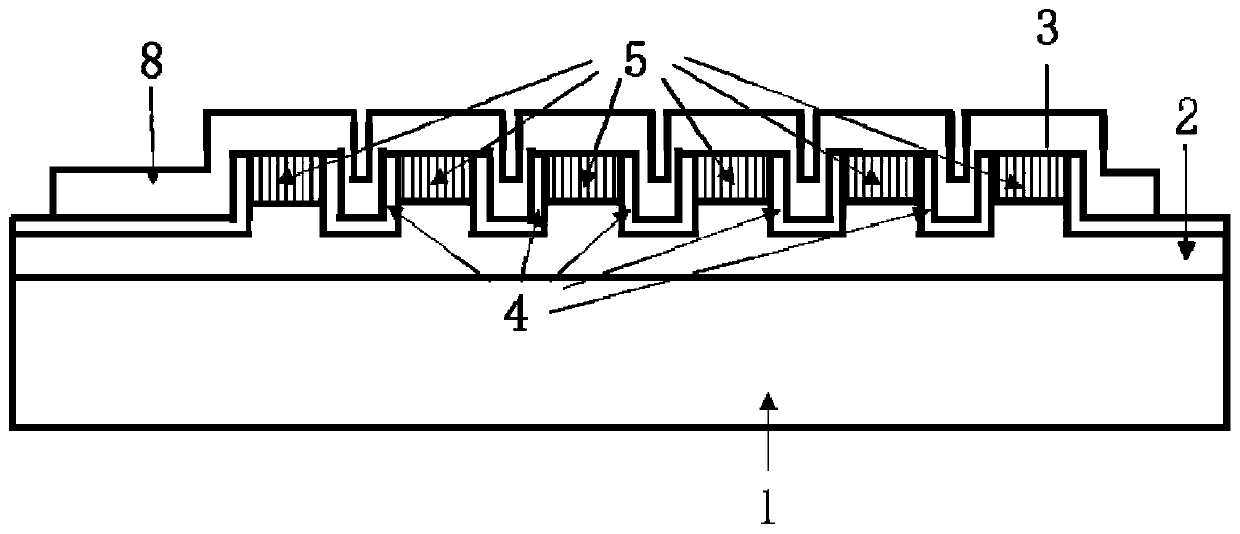
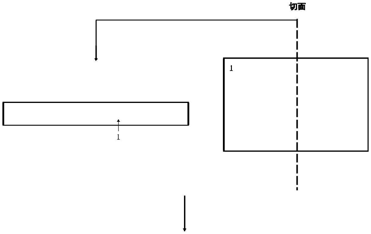
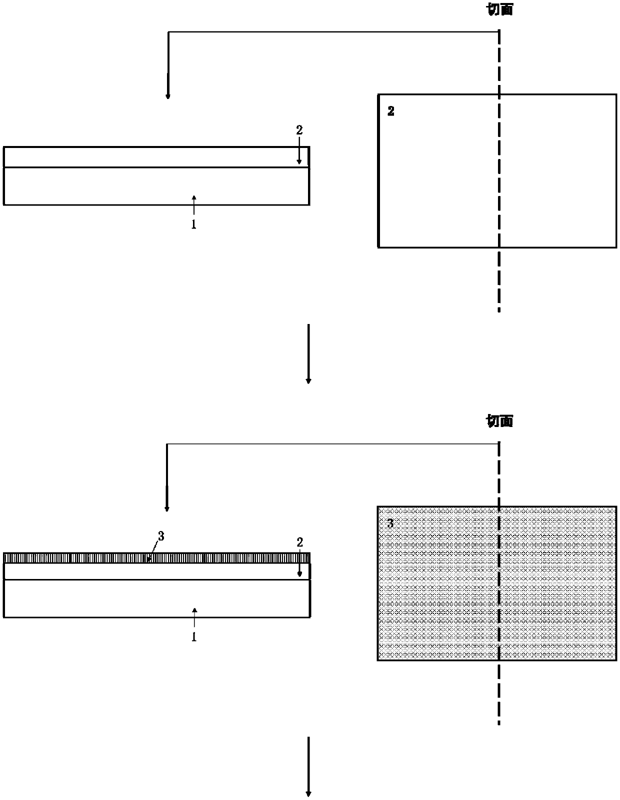
[0052] 1) The diamond substrate 1 grown by high temperature and high pressure (HPHT) technology is cleaned successively by using the standard cleaning process for diamond substrates, followed by inorganic and organic cleaning, and blown dry with nitrogen gas for later use.

[0053] 2) Deposit a single crystal diamond film 2 on the cleaned diamond substrate using microwave plasma vapor chemical deposition (MPCVD), the plasma power is 1kW, the chamber pressure is 100Torr, and the total gas flow is 500sccm, and the obtained single crystal diamond The thickness of the film is 1μm, the resistivity is greater than 100MΩ·cm, the root mean square surface roughness is less than 0.5nm, and the half-peak width of the Raman curve is less than 2cm -1 , XRD rocking curve half width less than 30arcsec.

[0054] 3) The diamond sample remains in the MPCVD chamber, t...

Embodiment 2

[0059] A method for preparing a bulk-doped diamond-based normally-off field-effect transistor, comprising the following steps:

[0060] 1) The diamond substrate 1 grown by high temperature and high pressure (HPHT) technology is cleaned successively by using the standard cleaning process for diamond substrates, followed by inorganic and organic cleaning, and blown dry with nitrogen gas for later use.

[0061] 2) Deposit a single crystal diamond film 2 on the cleaned diamond substrate using microwave plasma vapor chemical deposition (MPCVD), the plasma power is 1kW, the chamber pressure is 100Torr, and the total gas flow is 500sccm, and the obtained single crystal diamond The thickness of the film is 1μm, the resistivity is greater than 100MΩ·cm, the root mean square surface roughness is less than 0.5nm, and the half-peak width of the Raman curve is less than 2cm -1 , XRD rocking curve half width less than 30arcsec.

[0062] 3) The diamond sample is taken out and placed in a DC...

Embodiment 3

[0067] A method for preparing a bulk-doped diamond-based normally-off field-effect transistor, comprising the following steps:

[0068] 1) The diamond substrate 1 grown by high temperature and high pressure (HPHT) technology is cleaned successively by using the standard cleaning process for diamond substrates, followed by inorganic and organic cleaning, and blown dry with nitrogen gas for later use.

[0069] 2) Deposit a single crystal diamond film 2 on the cleaned diamond substrate using microwave plasma vapor chemical deposition (MPCVD), the plasma power is 1kW, the chamber pressure is 100Torr, and the total gas flow is 500sccm, and the obtained single crystal diamond The thickness of the film is 1μm, the resistivity is greater than 100MΩ·cm, the root mean square surface roughness is less than 0.5nm, and the half-peak width of the Raman curve is less than 2cm -1 , XRD rocking curve half width less than 30arcsec.

[0070] 3) The diamond sample is taken out and placed in the ...


PUM

PropertyMeasurementUnit
electrical resistivityaaaaaaaaaa
surface roughnessaaaaaaaaaa
carrier mobilityaaaaaaaaaa

Abstract

The invention discloses a bulk doped diamond-base normally-off field effect transistor and a preparation method thereof. The bulk doped diamond-base normally-off field effect transistor comprises a diamond substrate; a single crystal diamond epitaxial film is disposed on the diamond substrate; a bulk doped single crystal epitaxial film and an etched region are disposed on the single crystal diamond epitaxial film; the etched region is a high Schottky barrier terminal; the bulk doped single crystal epitaxial film is provided with a channel region; the channel region includes a bulk doped singlecrystal epitaxial film as a conductive channel and is a low Schottky barrier terminal; a source electrode and a drain electrode are arranged on both sides of the channel region; and a gate electrodeis disposed in the etched region and the channel region between the source electrode and the drain electrode. The normally-off field effect transistor uses a bulk doped epitaxial single crystal diamond material as the conductive channel so as to exert the advantages of high temperature resistance, radiation resistance and capability of operating in a vicious environment of a diamond material.

Description

Technical field [0001] The invention belongs to the technical field of semiconductor devices, and particularly relates to a normally-off diamond-based field effect transistor and a preparation method thereof. Specifically, it relates to a body-doped diamond-based normally-off field-effect transistor and a preparation method thereof. Background technique [0002] Semiconductor single crystal materials have gone through four generations of development. The first generation of Si and Ge semiconductors brought mankind into the information age, and also promoted the intelligence and informatization of electronic systems. The second generation of semiconductors (GaAs, InP, MCT, etc.) has brought us optoelectronic devices, power electronic devices, radio frequency electronic devices and space anti-radiation devices, etc., triggering revolutions in the information fields such as wireless communications and optical communications. The third generation of wide bandgap semiconductors ...

Claims


Application Information

Patent Timeline
Patent Type & Authority Patents(China)
IPC IPC(8): H01L27/095H01L29/16H01L29/167H01L21/338H01L29/812
CPCH01L27/095H01L29/1602H01L29/167H01L29/66045H01L29/8126
Inventor 王玮王宏兴问峰王艳丰张明辉林芳张景文卜忍安侯洵
Owner XI AN JIAOTONG UNIV
Why Eureka
Try Eureka