A short-wave/medium-wave/long-wave three-band infrared detector and its preparation method

An infrared detector, three-band technology, used in semiconductor devices, final product manufacturing, sustainable manufacturing/processing, etc., can solve problems such as the gap between InAsSb photoelectric infrared detectors, suppress tunneling dark current, reduce detection limits, The effect of high detection rate and practicality

Active Publication Date: 2022-05-06
YUNNAN NORMAL UNIV
View PDF2 Cites 0 Cited by
  • Summary
  • Abstract
  • Description
  • Claims
  • Application Information

AI Technical Summary

Problems solved by technology

[0005] There is a big gap in domestic research on InAsSb photoelectric infrared detectors compared with international ones

Method used


Image

  • A short-wave/medium-wave/long-wave three-band infrared detector and its preparation method
  • A short-wave/medium-wave/long-wave three-band infrared detector and its preparation method
  • A short-wave/medium-wave/long-wave three-band infrared detector and its preparation method

Examples


Embodiment 1

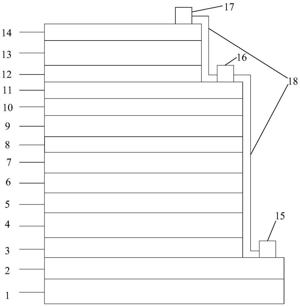
[0048]In the embodiment of the present invention, the degassed N-type GaSb(001) substrate is transferred into the growth chamber to heat up and remove the oxide layer. After the substrate temperature exceeds 370°C, the Sb protection beam is introduced, and the size of the Sb protection beam is at 10 -6 Torr level, real-time monitoring by RHEED, add 30°C to 620°C on the basis of the temperature 590°C when the deoxidation point appears on the substrate surface, and remove the oxide layer for 25 minutes.

[0049] In the embodiment of the present invention, the n-type doped GaSb buffer layer 2 is grown on the GaSb substrate 1 with a thickness of 1.1 μm. Among them, the Te doping concentration in the GaSb buffer layer is close to 2×10 18 cm -3 .

[0050] In the embodiment of the present invention, the n-type InAs / GaSb superlattice contact layer 3 is grown on the n-type doped GaSb buffer layer 2 with a thickness of 0.5 μm. This layer is composed of alternately grown GaSb barrier...

Embodiment 2

[0068] In the embodiment of the present invention, the degassed N-type GaSb(001) substrate is transferred into the growth chamber to heat up and remove the oxide layer. After the substrate temperature exceeds 370°C, the Sb protection beam is introduced, and the size of the Sb protection beam is at 10 -6 The Torr level is monitored in real time by REED. On the basis of the temperature of 600°C when the deoxidation point appears on the substrate surface, add 30°C, that is, 630°C, and deoxidize for 20 minutes.

[0069] In the embodiment of the present invention, the n-type doped GaSb buffer layer 2 is grown on the GaSb substrate 1 with a thickness of 0.92 μm. Among them, the Te doping concentration in the GaSb buffer layer is close to 2×10 18 cm -3 .

[0070] In the embodiment of the present invention, the n-type InAs / GaSb superlattice contact layer 3 is grown on the n-type doped GaSb buffer layer 2, and its thickness is 0.53 μm. This layer is composed of alternately grown Ga...

Embodiment 3

[0085] In the embodiment of the present invention, the degassed N-type GaSb(001) substrate is transferred into the growth chamber to heat up and remove the oxide layer. After the substrate temperature exceeds 370°C, the Sb protection beam is introduced, and the size of the Sb protection beam is at 10 -6 The Torr level is monitored in real time by REED. On the basis of the temperature of 600°C when the deoxidation point appears on the substrate surface, add 30°C, that is, 630°C, and deoxidize for 22 minutes.

[0086] In the embodiment of the present invention, the n-type doped GaSb buffer layer 2 is grown on the GaSb substrate 1 with a thickness of 0.88 μm. Among them, the Te doping concentration in the GaSb buffer layer is close to 2×10 18 cm -3 .

[0087] In the embodiment of the present invention, the n-type InAs / GaSb superlattice contact layer 3 is grown on the n-type doped GaSb buffer layer 2 with a thickness of 0.5 μm. This layer consists of alternately grown GaSb bar...


PUM

PropertyMeasurementUnit
thicknessaaaaaaaaaa
thicknessaaaaaaaaaa
thicknessaaaaaaaaaa

Abstract

The invention discloses a short-wave / medium-wave / long-wave three-band infrared detector, the structure of which includes a GaSb substrate, an epitaxial structure deposited on the GaSb substrate, a passivation layer, and a metal electrode, and the epitaxial structure is sequentially arranged from bottom to top Te-doped GaSb buffer layer, n-type InAs / GaSb superlattice contact layer, M-type InAs / GaSb / AlSb / GaSb / InAs superlattice hole blocking layer, p-type InAs / GaSb superlattice long-wave infrared absorption layer, p-type InAs / GaSb superlattice contact layer, p-type GaSb contact layer, p-type InAs / InAsSb superlattice contact layer, undoped InAs / InAsSb superlattice mid-wave infrared absorbing layer, n-type InAs / InAsSb superlattice contact layer, n-type GaSb contact layer, n-type InAs 0.91 Sb 0.09 Contact layer, undoped InAs 0.91 Sb 0.09 Short-wave infrared absorbing layer, p-type InAs 0.91 Sb 0.09 contact layer. The detector has P-π-M-N type InAs / GaSb superlattice, PIN type InAs / InAsSb superlattice and PIN type InAsSb heterostructure, with high detection rate, high responsivity, high quantum efficiency, low dark The advantages of low current and low crosstalk can improve the performance of infrared detectors.

Description

technical field [0001] The invention belongs to the field of semiconductor materials and devices, and relates to a short-wave / medium-wave / long-wave three-band infrared detector. Background technique [0002] Infrared detectors are widely used in military and civilian fields such as ballistic missile early warning, air-to-air missile seeker, lidar, night vision, communication, high-resolution satellite imaging, medicine, atmospheric monitoring, and industry. With the development of detection technology and the improvement of detection effect requirements, the current infrared detection technology is developing towards the direction of obtaining more target information, thus putting forward higher requirements for the performance of infrared detectors. At present, one of the important development directions of the third-generation infrared detectors at home and abroad is to realize multi-band simultaneous detection. If a detection system can obtain target information in multi...

Claims


Application Information

Patent Timeline
Patent Type & Authority Patents(China)
IPC IPC(8): H01L31/101H01L31/0352H01L31/0304H01L31/18
CPCH01L31/03046H01L31/035236H01L31/101H01L31/1844Y02P70/50
Inventor 郝瑞亭郭杰刘欣星常发冉李勇顾康
Owner YUNNAN NORMAL UNIV
Why Eureka
Try Eureka