A kind of preparation method of three-color infrared detector

A technology of infrared detector and infrared absorbing layer, which is applied in the direction of semiconductor devices, final product manufacturing, sustainable manufacturing/processing, etc., can solve the problems of not showing high performance, achieve the suppression of tunneling dark current, improve performance, and improve The effect of detecting the effect

Inactive Publication Date: 2018-02-16
YUNNAN NORMAL UNIV
View PDF3 Cites 0 Cited by
  • Summary
  • Abstract
  • Description
  • Claims
  • Application Information

AI Technical Summary

Problems solved by technology

However, due to the relatively high generated recombination (G-R) dark current of the devices fabricated by this material system, it did not show the expected high performance

Method used


Image

  • A kind of preparation method of three-color infrared detector
  • A kind of preparation method of three-color infrared detector
  • A kind of preparation method of three-color infrared detector

Examples


Embodiment 1

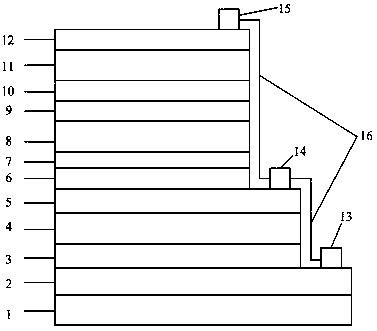
[0040] In the embodiment of the present invention, the degassed N-type GaSb (001) substrate is transferred into the growth chamber to remove the oxide layer by raising the temperature. After the substrate temperature exceeds 370 ° C, the Sb protection beam is introduced, and the size of the Sb protection beam is at 10 -6 Torr level, real-time monitoring by REED, 30°C is added to the temperature of 600°C when the deoxidation point appears on the substrate surface, that is, 630°C, and deoxidation is performed for 22 minutes.

[0041] In the embodiment of the present invention, the p-type doped GaSb buffer layer 2 is grown on the GaSb substrate 1 with a thickness of 1.1 μm. Among them, the Be doping concentration in the GaSb buffer layer is close to 2×10 18 cm -3 .

[0042] In the embodiment of the present invention, the p-type InAs / InAsSb superlattice contact layer 3 is grown on the p-type doped GaSb buffer layer 2 with a thickness of 0.677 μm. The layer consists of altern...

Embodiment 2

[0055] In the embodiment of the present invention, the degassed N-type GaSb (001) substrate is transferred into the growth chamber to remove the oxide layer by raising the temperature. After the substrate temperature exceeds 370 ° C, the Sb protection beam is introduced, and the size of the Sb protection beam is at 10 -6 Torr level, real-time monitoring by REED, on the basis of the temperature 600°C when the deoxidation point appears on the substrate surface, add 30°C, that is, 630°C, and deoxidize for 26 minutes.

[0056] In the embodiment of the present invention, the p-type doped GaSb buffer layer 2 is grown on the GaSb substrate 1 with a thickness of 0.88 μm. Among them, the Be doping concentration in the GaSb buffer layer is close to 2×10 18 cm -3 .

[0057] In the embodiment of the present invention, the p-type InAs / InAsSb superlattice contact layer 3 is grown on the p-type doped GaSb buffer layer 2 with a thickness of 0.677 μm. The layer consists of alternately gr...

Embodiment 3

[0070] In the embodiment of the present invention, the degassed N-type GaSb (001) substrate is transferred into the growth chamber to remove the oxide layer by raising the temperature. After the substrate temperature exceeds 370 ° C, the Sb protection beam is introduced, and the size of the Sb protection beam is at 10 -6 Torr level, real-time monitoring by REED, 30°C is added to the temperature of 600°C when the deoxidation point appears on the substrate surface, that is, 630°C, and deoxidation is carried out for 18 minutes.

[0071] In the embodiment of the present invention, the p-type doped GaSb buffer layer 2 is grown on the GaSb substrate 1 with a thickness of 1 μm. Among them, the Be doping concentration in the GaSb buffer layer is close to 2×10 18 cm -3 .

[0072] In the embodiment of the present invention, the p-type InAs / InAsSb superlattice contact layer 3 is grown on the p-type doped GaSb buffer layer 2 with a thickness of 0.677 μm. The layer consists of altern...


PUM


Abstract

The invention discloses a fabrication method of a three-color infrared detector. The structure of the three-color infrared detector comprises a GaSb substrate and an epitaxial structure, a passivation layer and a metal electrode which are deposited on the GaSb substrate, wherein the epitaxial structure sequentially comprises a Be-doped GaSb buffer layer, a p-type InAs / InAsSb superlattice contact layer, a non-doped InAs / InAsSb superlattice infrared absorption layer, an n-type InAs / InAsSb superlattice contact layer, a first n-type InAsSb contact layer, an AlAsSb electron barrier layer, a non-doped InAsSb infrared absorption layer, a second n-type InAsSb contact layer, an n-type low-temperature GaSb contact layer, a non-doped low-temperature GaSb infrared absorption layer and a p-type low-temperature GaSb contact layer (a cover layer) from bottom to top. The detector has PIN-type InAs / InAsSb superlattices, an NBN-type InAsSb heterojunction structure and a PIN-type low-temperature GaSb structure and has the advantages of high detection rate, low dark current, low crosstalk and the like, and the performance of the infrared detector can be improved.

Description

technical field [0001] The invention belongs to the field of semiconductor materials and devices, and relates to a three-color infrared detector. Background technique [0002] Due to its excellent performance, infrared detectors have been widely used in military and civilian fields such as intercontinental ballistic missile early warning, infrared guidance, night vision, communication, hyperspectral imaging, medicine, and atmospheric monitoring. With the development of detection technology and the improvement of detection requirements, the current infrared detection technology is developing towards the direction of obtaining more target information, thus putting forward higher requirements for the performance of infrared detectors. At present, one of the important development directions of the third-generation infrared detectors at home and abroad is to realize multi-band simultaneous detection. If a detection system can obtain target information in multiple bands, it can s...

Claims


Application Information

Patent Timeline
Patent Type & Authority Patents(China)
IPC IPC(8): H01L31/101H01L31/0352H01L31/0304H01L31/18
CPCH01L31/03046H01L31/035236H01L31/1013H01L31/1844Y02P70/50
Inventor 郝瑞亭任洋郭杰刘思佳赵其琛王书荣常发冉刘欣星
Owner YUNNAN NORMAL UNIV
Why Eureka
Try Eureka