A preparation method of a short-wave/medium-wave/long-wave three-band infrared detector

An infrared detector, three-band technology, applied in the direction of semiconductor devices, electrical components, circuits, etc., can solve the problems of incomplete replication of pre-set layer components and target components, low utilization rate of evaporation source materials, evaporation source pollution, etc. , to achieve the effects of suppressing generation-recombination dark current and tunneling dark current, reducing detection limit and improving performance

Inactive Publication Date: 2018-04-03
YUNNAN NORMAL UNIV
View PDF2 Cites 0 Cited by
  • Summary
  • Abstract
  • Description
  • Claims
  • Application Information

AI Technical Summary

Problems solved by technology

Among them, the quality of the film prepared by vacuum evaporation is high, but the biggest problem of this technology is the low utilization rate of the evaporation source material, and the pollution between the evaporation sources in the evaporation chamber is serious.
However, the prefabricated layer of copper, zinc, tin and sulfur prepared by vacuum sputtering is easy to control the film thickness, and there is no pollution of various targets in the chamber, but there are problems such as incomplete replication between the prefabricated layer components and target components, and poor reproducibility. question

Method used


Image

  • A preparation method of a short-wave/medium-wave/long-wave three-band infrared detector
  • A preparation method of a short-wave/medium-wave/long-wave three-band infrared detector
  • A preparation method of a short-wave/medium-wave/long-wave three-band infrared detector

Examples


Embodiment 1

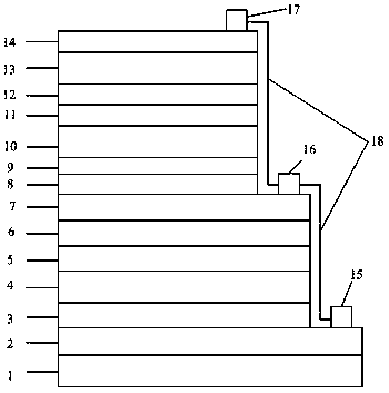
[0041] In the embodiment of the present invention, the degassed N-type GaSb (001) substrate is transferred into the growth chamber to remove the oxide layer by raising the temperature. After the substrate temperature exceeds 370 ° C, the Sb protection beam is introduced, and the size of the Sb protection beam is at 10 -6 Torr level, real-time monitoring by REED, on the basis of the temperature 600°C when the deoxidation point appears on the substrate surface, increase 30°C, that is, 630°C, and deoxidize for 25 minutes.

[0042] In the embodiment of the present invention, the n-type doped GaSb buffer layer 2 is grown on the GaSb substrate 1 with a thickness of 1.1 μm. Among them, the Te doping concentration in the GaSb buffer layer is close to 2×10 18 cm -3 .

[0043] In the embodiment of the present invention, the n-type InAs / GaSb superlattice contact layer 3 is grown on the n-type doped GaSb buffer layer 2 with a thickness of 0.5 μm. This layer is composed of alternatel...

Embodiment 2

[0058] In the embodiment of the present invention, the degassed N-type GaSb (001) substrate is transferred into the growth chamber to remove the oxide layer by raising the temperature. After the substrate temperature exceeds 370 ° C, the Sb protection beam is introduced, and the size of the Sb protection beam is at 10 -6 Torr level, real-time monitoring by REED, on the basis of the temperature 600°C when the deoxidation point appears on the substrate surface, add 30°C, that is, 630°C, and deoxidize for 20 minutes.

[0059] In the embodiment of the present invention, the n-type doped GaSb buffer layer 2 is grown on the GaSb substrate 1 with a thickness of 0.92 μm. Among them, the Te doping concentration in the GaSb buffer layer is close to 2×10 18 cm -3 .

[0060] In the embodiment of the present invention, the n-type InAs / GaSb superlattice contact layer 3 is grown on the n-type doped GaSb buffer layer 2, and its thickness is 0.53 μm. This layer is composed of alternately...

Embodiment 3

[0075] In the embodiment of the present invention, the degassed N-type GaSb (001) substrate is transferred into the growth chamber to remove the oxide layer by raising the temperature. After the substrate temperature exceeds 370 ° C, the Sb protection beam is introduced, and the size of the Sb protection beam is at 10 -6 Torr level, real-time monitoring by REED, 30°C is added to the temperature of 600°C when the deoxidation point appears on the substrate surface, that is, 630°C, and deoxidation is performed for 22 minutes.

[0076] In the embodiment of the present invention, the n-type doped GaSb buffer layer 2 is grown on the GaSb substrate 1 with a thickness of 0.88 μm. Among them, the Te doping concentration in the GaSb buffer layer is close to 2×10 18 cm -3 .

[0077] In the embodiment of the present invention, the n-type InAs / GaSb superlattice contact layer 3 is grown on the n-type doped GaSb buffer layer 2 with a thickness of 0.5 μm. This layer consists of alternat...


PUM


Abstract

The invention discloses a short wave / medium wave / long wave triple-band infrared detector, which structurally comprises a GaSb substrate, an epitaxial structure deposited on the GaSb structure, a passivation layer and metal electrodes, wherein the epitaxial structure sequentially comprises a Te-doped GaSb buffer layer, an n-type InAs / GaSb superlattice contact layer, an M-type InAs / GaSb / AlSb / GaSb / InAs superlattice hole blocking layer, a p-type InAs / GaSb superlattice long-wave infrared absorption layer, a p-type InAs / GaSb superlattice contact layer, a p-type GaSb contact layer (buffer layer), a p-type InAs / InAsSb superlattice contact layer, an un-doped InAs / InAsSb superlattice medium-wave infrared absorption layer, an n-type InAs / InAsSb superlattice contact layer, a first n-type InAsSb contact layer, an AlAsSb electronic barrier layer, an un-doped InAsSb short-wave infrared absorption layer and a second n-type InAsSb contact layer (cover layer) from bottom to top. The detector has a P-pi-M-N-type InAs / GaSb superlattice, a PIN-type InAs / InAsSb superlattice and an NBN-type InAsSb heterostructure, and has the advantages of high detection rate, low dark current, low crosstalk and the like, and the performance of the infrared detector can be improved.

Description

technical field [0001] The invention belongs to the field of semiconductor materials and devices, and relates to a short-wave / medium-wave / long-wave three-band infrared detector. Background technique [0002] A novel quaternary compound semiconductor copper zinc tin sulfur selenide (Cu 2 ZnSn(S,Se) 4 , abbreviated as CZTSSe) and copper indium gallium selenide (CuInGaSe 2 , abbreviated CIGS) all belong to the chalcopyrite structure, the difference is that CZTSSe replaces gallium (Ga) and indium (In) in CIGS with tin (Sn) and zinc (Zn), and replaces selenium (Se) with sulfur (S). , does not contain rare and noble elements (In and Ga) and toxic elements (Se). Compared with CIGS, the band gap (1.1~1.5eV) of CZTSSe matches the solar spectrum more closely, and CZTSSe has the same excellent light absorption coefficient as CIGS (greater than 10 4 cm -1 ), its theoretical conversion efficiency can reach 32.2%, and CZTSSe is generally considered to be one of the best choices for a...

Claims


Application Information

Patent Timeline
Patent Type & Authority Patents(China)
IPC IPC(8): H01L31/101H01L31/11
CPCH01L31/1013H01L31/11
Inventor 郝瑞亭任洋郭杰刘思佳赵其琛王书荣常发冉刘欣星
Owner YUNNAN NORMAL UNIV
Why Eureka
Try Eureka