Two-color infrared detector material and its preparation method
An infrared detector and epitaxy technology, which is applied in the field of materials, can solve the problems of infrared target contrast reduction and difficulty in identification, and achieve the effects of reducing detection limits, improving resolution, and improving detection effects
- Summary
- Abstract
- Description
- Claims
- Application Information
AI Technical Summary
Problems solved by technology
Method used
Image
Examples
Embodiment 1
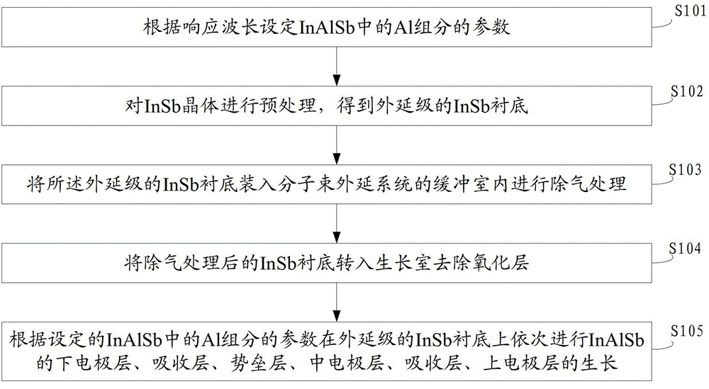
[0045] Embodiments of the present invention provide a method for preparing a two-color infrared detector material, such as figure 1 As shown, the method includes:
[0046] S101, setting the parameters of the Al component in InAlSb according to the response wavelength;
[0047] The response wavelength includes MW 1 band and MW 2 band, the wavelength range corresponding to the MW 1 band is 3.4-4.0 μm, and the wavelength range corresponding to the MW 2 band is 4.4-5.0 μm.
[0048] S102, pretreating the InSb crystal to obtain an epitaxial-level InSb substrate;
[0049] The steps of preprocessing the InSb crystal to obtain an epitaxial-level InSb substrate specifically include:
[0050] Use the pulling method to prepare 2inch (inch) InSb crystals, and cut the InSb crystals into (001) crystal plane InSb wafers;
[0051] After the InSb (001) wafer is roughly ground, it is rounded and chamfered to prepare a 2-inch InSb substrate;
[0052] After the InSb substrate is polished and p...
Embodiment 2
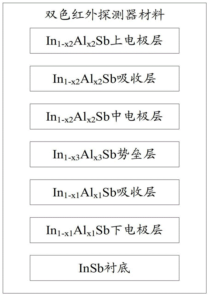
[0073] An embodiment of the present invention provides a two-color infrared detector material, such as figure 2 As shown, the two-color infrared detector material is a two-color infrared detector material obtained according to any of the above-mentioned methods, and the two-color infrared detector material comprises in turn: InSb substrate, In 1-x1 Al x1 Sb lower electrode layer, In 1-x1 Al x1 Sb absorption layer, In 1-x3 Al x3 Sb barrier layer, In 1-x2 Al x2 Sb middle electrode layer, In 1-x2 Al x2 Sb absorber layer and In 1-x2 Al x2 Sb upper electrode layer;
[0074] in,
[0075] The In 1-x1 Al x1 The thickness of the growth of the Sb lower electrode layer is 0.5-3μm, and the n-type doping concentration is 2×10 17 -6×10 18 cm -3 cm -3 ;
[0076] The In1- x1 Al xl The thickness of Sb absorbing layer growth is 0.5-6μm, without doping, and the concentration is controlled at 2×10 14 -5×10 16 cm -3 ;
[0077] The In 1-x3 Al x3The thickness of Sb barrier...
PUM
| Property | Measurement | Unit |
|---|---|---|
| wavelength | aaaaa | aaaaa |
| thickness | aaaaa | aaaaa |
| thickness | aaaaa | aaaaa |
Abstract
Description
Claims
Application Information

