Organic light-emitting diode (OLED) display panel and manufacturing method thereof

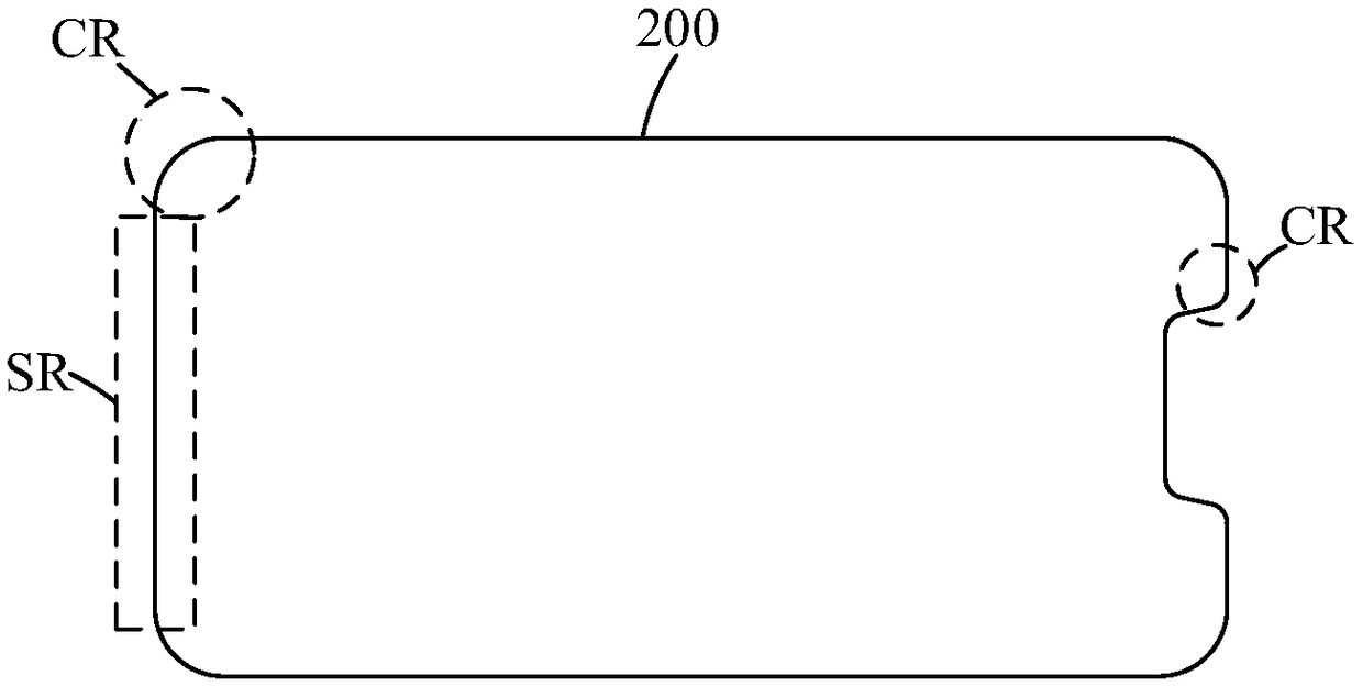
A technology for light-emitting diodes and display panels, which is applied in the manufacture of semiconductor/solid-state devices, electrical components, and electrical solid-state devices, etc., and can solve the problems of complex shapes, inability to obtain water and oxygen protection for OLED devices, and the number and shape of CRs in the corner areas of the special-shaped screen 200. complex issues

Active Publication Date: 2019-02-01
WUHAN CHINA STAR OPTOELECTRONICS SEMICON DISPLAY TECH CO LTD
View PDF4 Cites 24 Cited by
  • Summary
  • Abstract
  • Description
  • Claims
  • Application Information

AI Technical Summary

Problems solved by technology

figure 1 The retaining wall shown has four corner regions CR, figure 2 The number and shape of the corner region CR in the special-shaped screen 200 shown are more complicated.
[0006] Since the shape of the corner region CR is relatively more complex than that of the straight region SR, there is a problem in the prior art that the organic layer of the thin-film packaging structure overflows from the corner region CR, resulting in water and oxygen intrusion, OLED devices cannot obtain good water and oxygen protection, and reduce the Lifespan of OLED Displays
Due to the large number of CRs in the corner area of ​​the special-shaped screen 200, the problem of overflow of the organic layer of the thin-film packaging structure is more serious

Method used


Image

  • Organic light-emitting diode (OLED) display panel and manufacturing method thereof
  • Organic light-emitting diode (OLED) display panel and manufacturing method thereof
  • Organic light-emitting diode (OLED) display panel and manufacturing method thereof

Examples


Embodiment Construction

[0033] In order to make the purpose, technical solution and effect of the present application more clear and definite, the present application will be further described in detail below with reference to the accompanying drawings and examples. It should be understood that the specific embodiments described here are only used to explain the present application, and the word "embodiment" used in the description of the present application is intended to be used as an example, illustration or illustration, and is not intended to limit the present application.

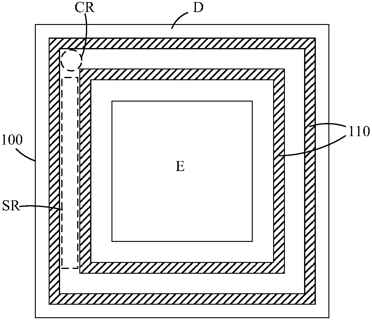
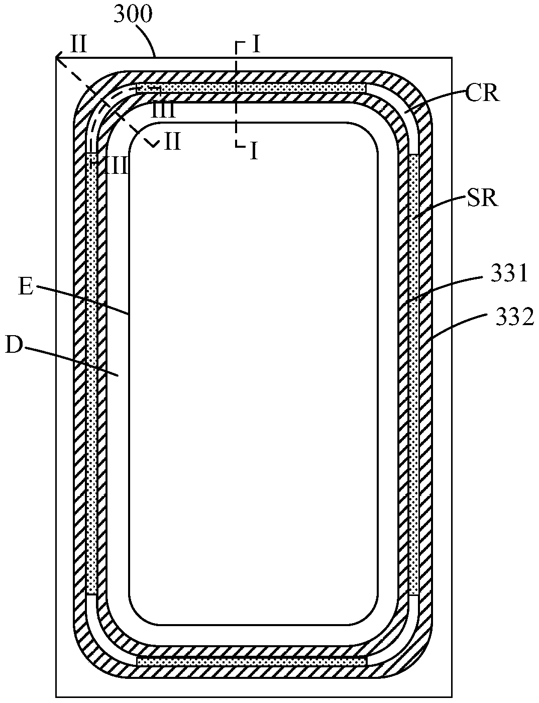
[0034] image 3 A schematic diagram of an organic light emitting diode (OLED) display panel 300 according to the present application is shown. Figure 4 show image 3 Sectional view along the dotted line I-I. Figure 5 show image 3 The sectional view along the dotted line II-II. Figure 6 show image 3 Sectional view along the dotted line III-III.

[0035] The OLED display panel 300 includes a non-display area D and a...


PUM


Abstract

The invention relates to an OLED display panel and a manufacturing method thereof. The OLED display panel comprises a TFT array substrate, organic light emitting units, a first retaining wall, a second retaining wall, a groove and a film packaging structure. The organic light emitting units are arranged in the display region, and the first and second barrier walls are arranged in the non-display region. The groove is formed in a position corresponding to a gap between the first and second barrier walls, and arranged in a laminated structure of an insulating layer of the TFT array substrate andincludes an exposed opening. The film packaging structure covers the component. Especially, the groove is arranged in a straight side area, and thus, a height difference is formed between the straight side area and a corner area in the TFT array substrate. Thus, the risk that an organic layer of the film packaging structure is overflow in the corner area can be reduced.

Description

technical field [0001] The present application relates to a display technology, in particular to an organic light emitting diode (organic light emitting diode) display panel and a manufacturing method thereof. Background technique [0002] Compared with a liquid crystal display (LCD), the organic light emitting diode display has the biggest advantage that the OLED display can realize flexible display. However, OLED devices are particularly sensitive to water and oxygen. In order to prevent the intrusion of water and oxygen while achieving the effect of flexible display, the traditional process uses a thin-film packaging structure to mold the OLED device. [0003] Generally speaking, the thin-film packaging structure is composed of overlapping organic layers and inorganic layers. The organic layer in the thin-film packaging structure has a certain degree of fluidity. In order to limit it to a certain area, a circle or Multi-circle retaining wall (dam). [0004] figure 1 A ...

Claims


Application Information

Patent Timeline
Patent Type & Authority Applications(China)
IPC IPC(8): H01L27/12H01L27/32H01L51/52H01L51/56H01L21/84
CPCH01L27/1218H01L27/1262H10K59/1213H10K50/844H10K59/1201H10K71/00
Inventor 曹君徐湘伦
Owner WUHAN CHINA STAR OPTOELECTRONICS SEMICON DISPLAY TECH CO LTD
Why Eureka
Try Eureka