Pixel circuit and display substrate

A pixel circuit and level technology, which is applied in the field of pixel circuits and display substrates, can solve problems such as the influence of pixel circuit crosstalk, and achieve the effects of reducing changes, improving display quality, and reducing the influence of crosstalk.

Active Publication Date: 2019-02-05
BOE TECH GRP CO LTD
View PDF9 Cites 7 Cited by
  • Summary
  • Abstract
  • Description
  • Claims
  • Application Information

AI Technical Summary

Problems solved by technology

[0004] The present invention at least partly solves the problem that existing pixel circuits are easily affected by crosstalk, and provides a pixel circuit and a display substrate that can reduce crosstalk effects

Method used


Image

  • Pixel circuit and display substrate
  • Pixel circuit and display substrate
  • Pixel circuit and display substrate

Examples


Embodiment 1

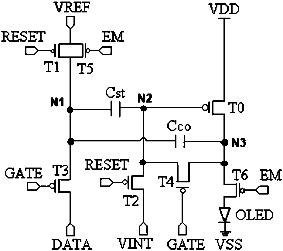
[0051] Such as Figure 2 to Figure 4 As shown, this embodiment provides a pixel circuit, including:

[0052] a light emitting unit for emitting light during the light emitting phase;

[0053] The storage unit is configured such that it is electrically connected to the first level terminal VREF and the driving unit during the light-emitting phase, and provides a driving level to the driving unit according to the level of the first level terminal VREF;

[0054] The driving unit is configured such that it is electrically connected to the first power supply terminal VDD, the light emitting unit, and the storage unit during the light emitting stage, and controls the light emitting brightness of the light emitting unit according to the driving level;

[0055] The compensation unit is configured to be electrically connected to the storage unit and the driving unit during the light-emitting phase, and to reduce the change degree of the driving level when the level of the first level ...

Embodiment 2

[0099] Such as Figure 5 , Figure 6 As shown, this embodiment provides a display substrate (such as an array substrate), which includes:

[0100] A plurality of pixel units, each of which is provided with one of the above-mentioned pixel circuits;

[0101] A plurality of first leads, each of which is connected to the first level terminals of a plurality of pixel circuits;

[0102] A plurality of second leads overlapping the first leads.

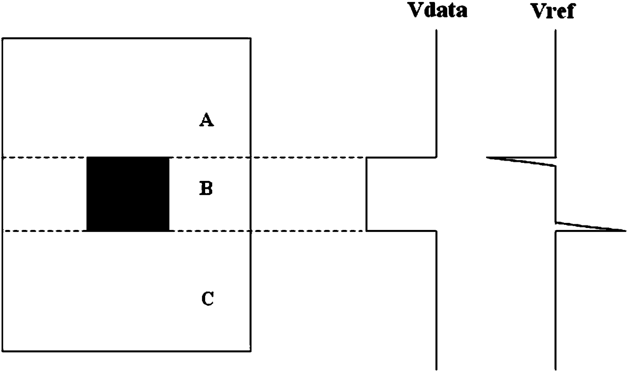
[0103] That is to say, the above pixel circuit can be used in a display substrate as a light emitting structure in each pixel unit. Wherein, the first level end of the pixel circuit can be powered through the first lead wire; of course, the reset end, control end, gate line end, data line end, second level end, first power supply end, and second power supply end in the pixel circuit etc., and should also be powered through corresponding leads, which will not be described in detail here.

[0104] The display substrate also has a second l...

Embodiment 3

[0120] This embodiment provides a display device, which includes the above-mentioned display substrate.

[0121] Specifically, the display device can be any product with a display function such as a liquid crystal display panel, an organic light-emitting diode (OLED) display panel, an electronic paper, a mobile phone, a tablet computer, a television set, a monitor, a notebook computer, a digital photo frame, a navigator, or the like. part.


PUM


Abstract

The present invention provides a pixel circuit and a display substrate and belongs to the technical field of pixel circuits. With the pixel circuit and the display substrate adopted, the problem thatan existing pixel circuit is susceptible to crosstalk can be partially solved. The pixel circuit of the present invention comprises a light emitting unit, a storage unit, a driving unit, and a compensation unit; the light emitting unit is used for emitting light during a light emitting phase; the storage unit is configured to be electrically connected with a first electric level end and the driving unit in the light emitting phase, and provide a driving electric level for the driving unit according to the electric level of the first electric level end; the driving unit is configured to be electrically connected with a first power source end, the light emitting unit and the storage unit in the light emitting phase, and control the light emitting brightness of the light emitting unit according to the driving electric level; the compensation unit is configured to be electrically connected with the storage unit and the driving unit in the light emitting phase and reduce the change degree of the driving electric level when the electric level of the first electric level end jumps.

Description

technical field [0001] The invention belongs to the technical field of pixel circuits, and in particular relates to a pixel circuit and a display substrate. Background technique [0002] In a display panel (such as an organic light-emitting diode display panel), due to the limitation of the layout design, there must be overlap between different leads, that is, there is a parasitic capacitance (coupling capacitance). Therefore, when the level of a lead wire jumps, the levels of other lead wires will also change due to induction, thereby affecting the display (crosstalk). [0003] For example, in a display panel, the reference level is supplied to all pixel units and is used to maintain the level at one end of the storage capacitor during the light-emitting phase, so that the other end of the storage capacitor can provide a stable driving level to the gate of the drive transistor. , so that the pixel unit can emit light stably according to the required brightness. The displa...

Claims


Application Information

Patent Timeline
Patent Type & Authority Applications(China)
IPC IPC(8): G09G3/3208
CPCG09G3/3208G09G2320/0626G09G3/3233G09G3/3225G09G2300/0819G09G2300/0852G09G2300/0861G09G2310/0262G09G2310/0245G09G2300/0426G09G2300/0876G09G3/32G09G3/3266G09G3/3275G09G2300/043G09G2320/0209
Inventor 玄明花
Owner BOE TECH GRP CO LTD
Why Eureka
Try Eureka