A backlight module, manufacturing method thereof, and display device

A technology of backlight module and manufacturing method, which is applied in the direction of semiconductor devices, electrical components, circuits, etc., and can solve problems such as defective stars in the sky

Active Publication Date: 2020-07-24
XIAMEN TIANMA MICRO ELECTRONICS
View PDF2 Cites 0 Cited by
  • Summary
  • Abstract
  • Description
  • Claims
  • Application Information

AI Technical Summary

Problems solved by technology

[0005] In view of this, the present invention provides a backlight module, a manufacturing method thereof, and a display device, so as to solve the problem of the bad phenomenon of starry sky in the display process of the backlight module in the prior art

Method used


Image

  • A backlight module, manufacturing method thereof, and display device
  • A backlight module, manufacturing method thereof, and display device
  • A backlight module, manufacturing method thereof, and display device

Examples


Embodiment Construction

[0035] As mentioned in the background technology section, in the prior art, the backlight module formed by Mini LED is prone to starry sky phenomenon during the display process.

[0036] The reason that inventor finds above-mentioned phenomenon occurs is:

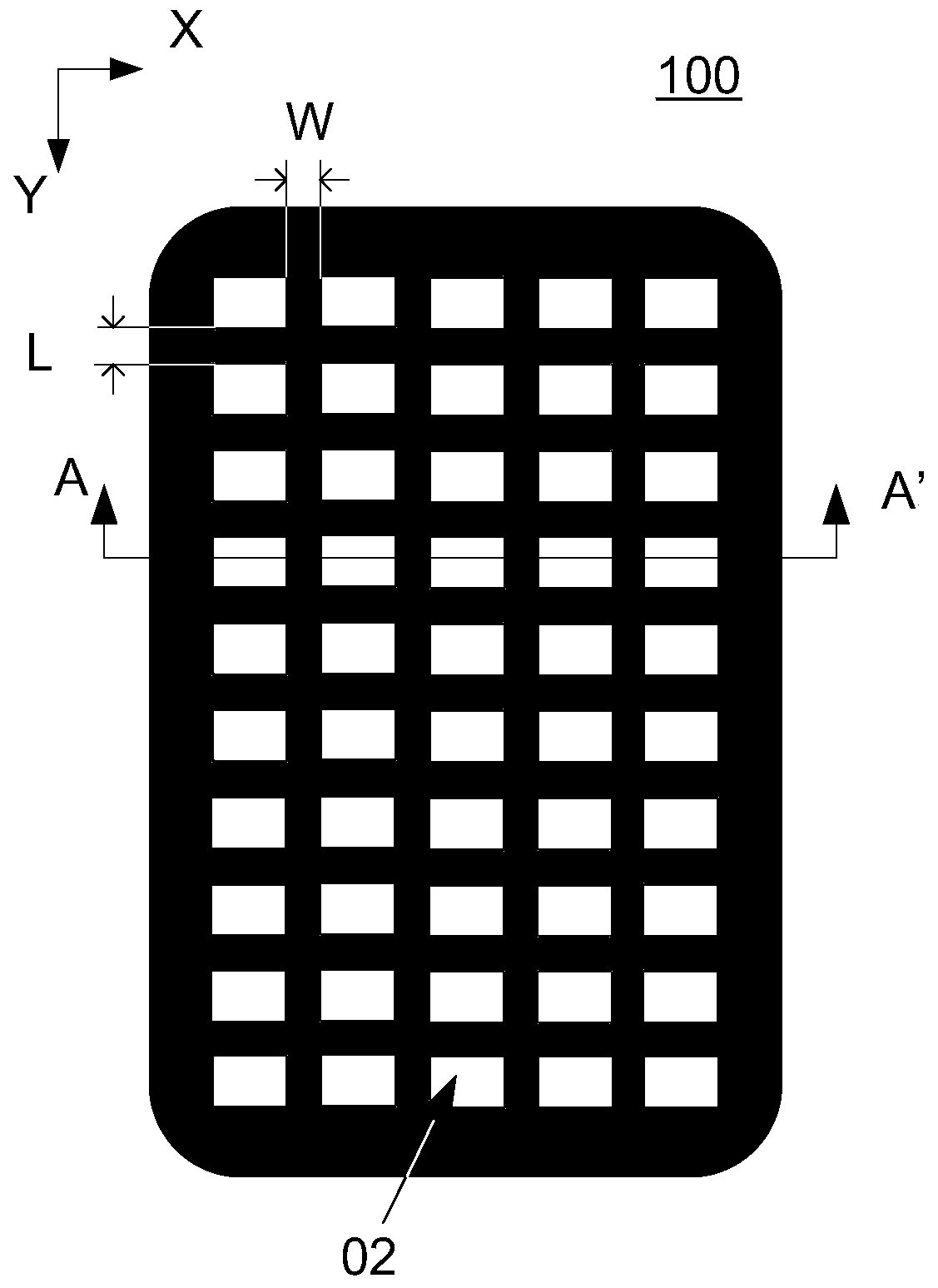
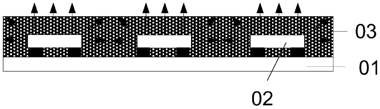
[0037] See figure 1 , figure 1 A schematic diagram of the top view structure of a display device provided for the prior art; in the display device 100, there will be a certain distance between adjacent LED chips 02, for example, there is a first gap between two adjacent LED chips 02 in the X direction. The spacing W, and the second spacing L between two adjacent LED chips 02 in the Y direction. See figure 2 , figure 2 for along figure 1 The cross-sectional schematic diagram of the backlight module of the line AA' in the middle; wherein, the LED backlight module includes a PCB board 01, a number of LED chips 02 are arranged on the PCB board 01, a fluorescent film 03 is arranged on the LED chip 02, and the light emitti...


PUM


Abstract

The application provides a backlight module, a manufacturing method thereof and a display device. The backlight module comprises a substrate and a plurality of LED chip structures arrayed on the substrate. Each LED chip structure includes first and second LED chip structures stacked, and a reflecting layer between the first and second LED chip structures, the reflecting layer reflects light, opposite to the surface of the substrate and emitted by the first LED chip structure between the substrate and the second LED chip structure, and the light exits from the side of the first LED chip structure. On one hand, the reflecting layers compensate lateral emission quantity of the light from the front of the first LED chip structures; on the other hand, the added LED chip structures help increaselateral emission quantity of the LED chip structures at the premise that the light emitted from the front of the LED chip structures has unchanged brightness. Both the two aspects weaken the starry effect and even thoroughly eliminate the starry effect.

Description

technical field [0001] The invention relates to the field of display technology, in particular to a backlight module, a manufacturing method thereof, and a display device. Background technique [0002] With the development of LED (Light-Emitting Diode, light-emitting diode) technology, the size of the LED light source used in the backlight module is getting smaller and smaller, and Mini LED is gradually used as the light source in the backlight module. Mini LED is called Micro The predecessor of LED (Micro Light Emitting Diode, Micro Light Emitting Diode), the size is about 50 microns to 60 microns. [0003] Mini LED is an emerging branch of the current display screen. Through this technology, the local dimming (Local Dimming) design of the direct-lit backlight module can be realized, and the screen effect of high dynamic range (HDR) can be achieved, making the picture more delicate. At the same time, it provides a high-brightness surface light source to improve the bright...

Claims


Application Information

Patent Timeline
Patent Type & Authority Patents(China)
IPC IPC(8): H01L25/075H01L33/10H01L33/52H01L33/50
CPCH01L25/0753H01L33/10H01L33/502H01L33/52
Inventor 黄阿海
Owner XIAMEN TIANMA MICRO ELECTRONICS
Why Eureka
Try Eureka