Cellular structure and power device

A technology of power devices and cells, which is applied in the direction of electrical components, semiconductor devices, circuits, etc., can solve the problems of limited avalanche tolerance of devices, and achieve the effect of improving avalanche tolerance and improving avalanche tolerance

Pending Publication Date: 2019-02-12
NANJING HRM SEMICON CO LTD
View PDF0 Cites 1 Cited by
  • Summary
  • Abstract
  • Description
  • Claims
  • Application Information

AI Technical Summary

Problems solved by technology

At present, there are two common cell designs, one is a bar grid design, and the other is a square design, and the avalanche tolerance of devices in both designs is limited.

Method used


Image

  • Cellular structure and power device
  • Cellular structure and power device
  • Cellular structure and power device

Examples


Embodiment Construction

[0014] The present invention will be further illustrated below in conjunction with the accompanying drawings and specific embodiments. This embodiment is implemented on the premise of the technical solution of the present invention. It should be understood that these embodiments are only used to illustrate the present invention and are not intended to limit the scope of the present invention.

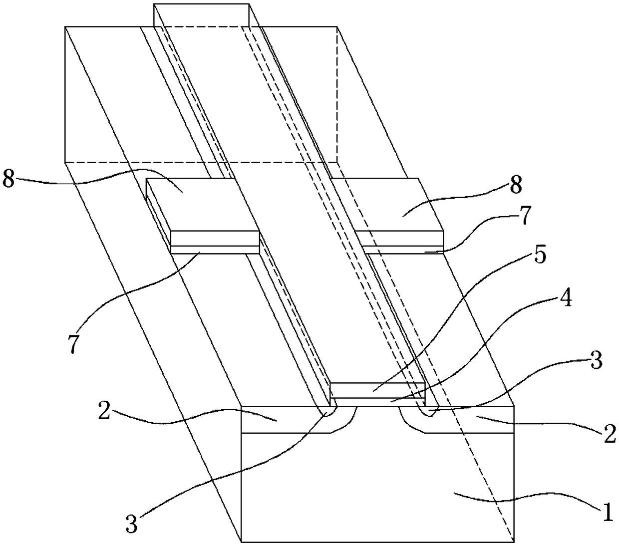
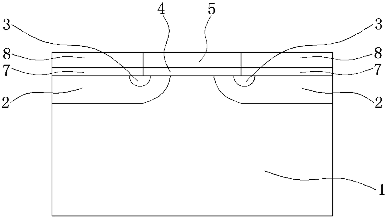
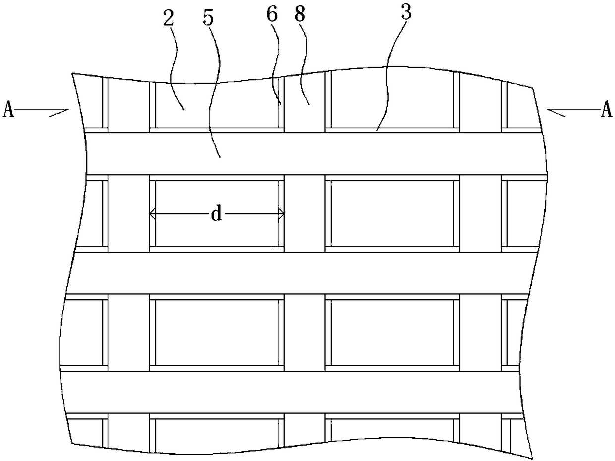
[0015] Such as Figures 1 to 4 As shown, the embodiment of the present invention provides a cell structure, the cell includes an N-epitaxial layer 1 and two P-wells 2 arranged on the upper side of the N-epitaxial layer 1, and the two P-wells 2 are arranged to The axial midline of the N-epitaxial layer 1 is arranged symmetrically, and two P-wells 2 are arranged at intervals, and the two are separated by a part of the N-epitaxial layer 1 . The upper side of the two P-wells 2 is respectively provided with the first N+ well 3, the upper side of the inner end of the P-well 2, the inner upper...


PUM

PropertyMeasurementUnit
Widthaaaaaaaaaa

Abstract

The invention discloses a cellular structure and a power device. A cell comprises an N-epitaxial layer and two P-traps symmetrically arranged on the upper side of the epitaxial layer at an interval, afirst N+ trap is arranged on the inner upper side of each P-trap, a first gate oxide layer covers each of the inner-end upper side of each P-trap, the inner upper side of each first N+ trap and the upper side of the N-epitaxial layer between the P-traps, a first polycrystalline strip is arranged on the upper side of each gate oxide layer, two second N+ traps are transversely arranged on the P-traps on two sides of the middle of the first polycrystalline strip at an interval, second gate oxide layers arranged on the inner upper sides of the two second N+ traps and the upper side of the P-trapbetween the two second N+ traps, and a second polycrystalline layer is arranged on the upper side of each second gate oxide layer. Through structural improvement, avalanche current orientation can beguided, so that avalanche tolerance is improved. After being improved by the scheme, the avalanche tolerance of the device can be improved by higher than 50% generally.

Description

technical field [0001] The invention relates to the field of semiconductor devices, in particular to a cellular structure and a power device. Background technique [0002] VDMOS (Vertical Double-diffused Metal Oxide Semiconductor) devices have the advantages of fast switching speed, low switching loss, high input impedance, voltage drive, high frequency, etc., and have been widely accepted and used by the market. In the application of VDMOS devices, an important indicator is the avalanche tolerance. The higher the avalanche tolerance, the wider the application range. At present, there are two common cell designs, one is a bar grid design, and the other is a square design. Both designs have limited avalanche tolerance. With the continuous development of VDMOS devices, its structure has been continuously improved to improve the avalanche tolerance as much as possible, thereby improving the impact resistance. Contents of the invention [0003] The object of the present inve...

Claims


Application Information

Patent Timeline
IPC IPC(8): H01L29/06H01L29/78
CPCH01L29/0623H01L29/0696H01L29/7802
Inventor 胡兴正陈虞平刘海波
Owner NANJING HRM SEMICON CO LTD
Why Eureka
Try Eureka