Power semiconductor device

A semiconductor and power technology, applied in the field of power semiconductor devices, can solve the problem that MOSFET is easy to be damaged

Inactive Publication Date: 2012-04-11
KK TOSHIBA
View PDF7 Cites 1 Cited by
  • Summary
  • Abstract
  • Description
  • Claims
  • Application Information

AI Technical Summary

Problems solved by technology

As a result, the current is concentrated and the MOSFET becomes easily damaged

Method used


Image

  • Power semiconductor device
  • Power semiconductor device
  • Power semiconductor device

Examples


no. 1 approach

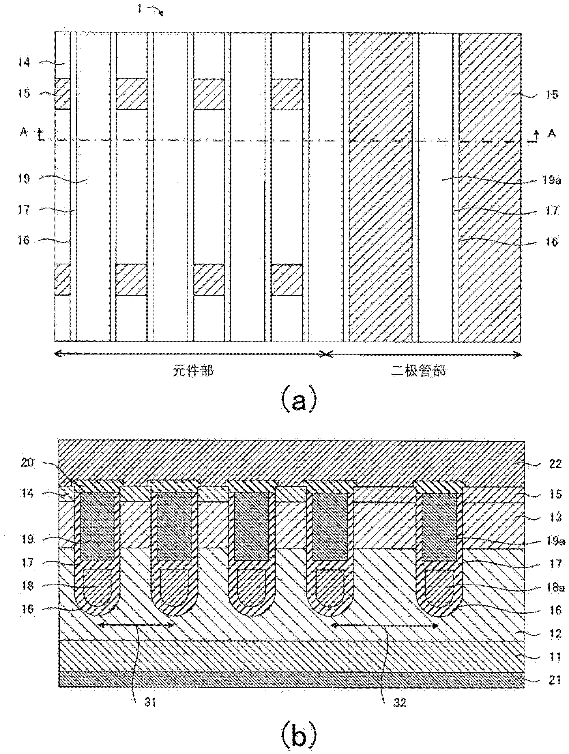
[0016] refer to figure 1 and figure 2 A semiconductor device according to an embodiment of the present invention will be described. figure 1 (a) means to remove figure 1 (b) The top view of the state after two layers of the upper end (upper part of the paper), figure 1 (b) is along figure 1 (a) Cross-sectional view along line A-A.

[0017] like figure 1 As shown, the semiconductor device 1 has: an element portion including a region having an n-channel vertical MOSFET; and a diode portion including a region including a diode adjacent to the element portion. exist figure 1 , the left side of the page is the element part, and the right side of the page connected to the element part is the diode part.

[0018] The element portion has an n+ type semiconductor substrate 11 containing, for example, single crystal silicon and serving as a first semiconductor layer of the first conductivity type. On the first main surface (upper surface) of the n+ type semiconductor substrate ...

no. 2 approach

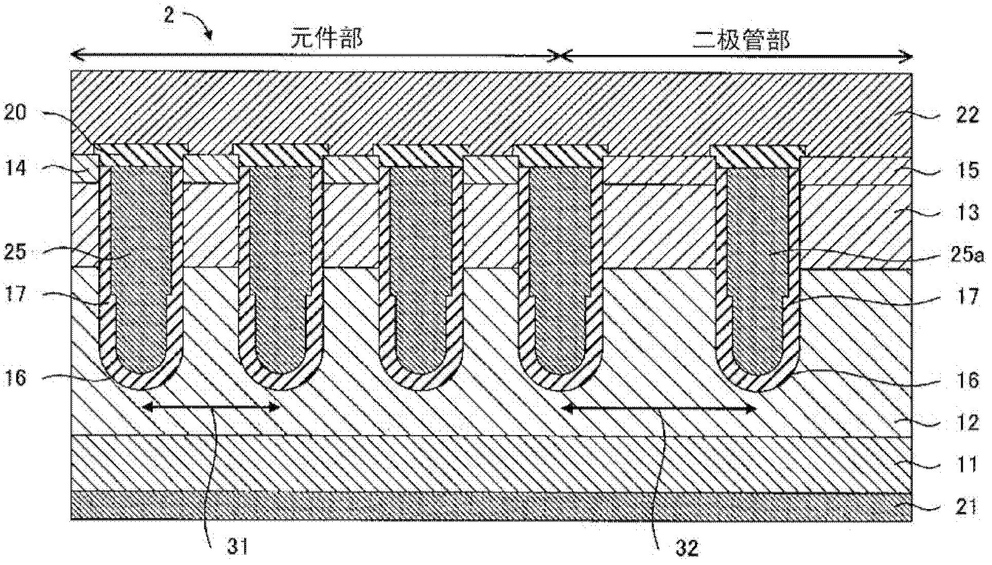
[0042] refer to image 3 A semiconductor device according to an embodiment of the present invention will be described. image 3 With figure 1 (b) Corresponding cross-sectional view. Compared with the semiconductor device 1 of the first embodiment, the difference is that a gate electrode having a narrower stepped structure is provided at the bottom of the trench. In addition, the same code|symbol is attached|subjected to the same component as 1st Embodiment, and the description is abbreviate|omitted.

[0043] like image 3 As shown, the semiconductor device 2 is provided with a gate electrode 25 in the element portion. The gate electrode 25 is formed from the top to the bottom of the trench 16 via the insulating film 17 on the inner surface of the trench 16 and contains, for example, conductive polysilicon. In the diode portion, a gate electrode member 25 a is provided similarly to the gate electrode 25 . Other configurations of the semiconductor device 2 are the same as t...


PUM


Abstract

The invention provides a semiconductor device, which includes an element unit including a vertical-type MOSFET and a diode unit adjacent to the element unit. The vertical-type MOSFET includes a first semiconductor layer of a first conductivity type, a second semiconductor layer of a first conductivity type, a third semiconductor layer of a second conductivity type, a fourth semiconductor layer of a first conductivity type, a fifth semiconductor layer of a second conductivity type; an insulator covering inner surfaces of a plurality of trenches penetrating from the surface of the fourth semiconductor layer or the fifth semiconductor layer to the second semiconductor layer through the third semiconductor layer, the adjacent trenches being provided with a first interval in between; a first embedded conducting layer, a second embedded conducting layer, a layer insulation film, a first main electrode and a second main electrode. The diode unit includes a first semiconductor layer, a second semiconductor layer, a third semiconductor layer, a fifth semiconductor layer, an insulator, a first embedded conducting layer, a second embedded conducting layer, a layer insulation film, a first main electrode and a second main electrode, the adjacent trenches being provided with a second interval in between.

Description

[0001] This application is based on and claims the priority of the prior patent application No. 2010-209160 filed in Japan on September 17, 2010, and the entire content of the prior application is included in the present application. technical field [0002] Embodiments of the present invention relate to a power semiconductor device. Background technique [0003] Regarding the use of power semiconductor devices including MOSFETs (Metal Oxide Silicon Field Effect Transistor: Metal Oxide Semiconductor Field Effect Transistors), in addition to the high-current, high-voltage switching power supply market, in recent years, notebook PCs have moved The market for energy-saving switches for communication equipment is also rapidly increasing. Power semiconductor devices are used in power management circuits, safety circuits for lithium-ion batteries, and the like. Therefore, power semiconductor devices are designed to achieve low-voltage driving, low on-resistance, and reduction in ...

Claims


Application Information

Patent Timeline
IPC IPC(8): H01L29/06H01L29/78
CPCH01L29/7805H01L29/407H01L29/0626H01L29/7808H01L29/4238H01L29/42368H01L29/0696H01L29/4236H01L29/7813H01L27/0727
Inventor 川口雄介
Owner KK TOSHIBA
Why Eureka
Try Eureka