Super junction structure and manufacturing method thereof

A superjunction, N-type technology, used in semiconductor/solid-state device manufacturing, semiconductor devices, electrical components, etc.

Active Publication Date: 2020-06-26
SHENZHEN SANRISE TECH CO LTD
View PDF8 Cites 2 Cited by
  • Summary
  • Abstract
  • Description
  • Claims
  • Application Information

AI Technical Summary

Problems solved by technology

However, in order to speed up the filling of the epitaxy in the trench, the trench will be made into a certain inclination angle. At this time, at different horizontal positions of the PN column, the ratio of the width of the P column to the width of the N column will change. Therefore, if it is assumed that N If the...

Method used


Image

  • Super junction structure and manufacturing method thereof
  • Super junction structure and manufacturing method thereof
  • Super junction structure and manufacturing method thereof

Examples


no. 1 example

[0055] The super junction structure of the first embodiment of the present invention:

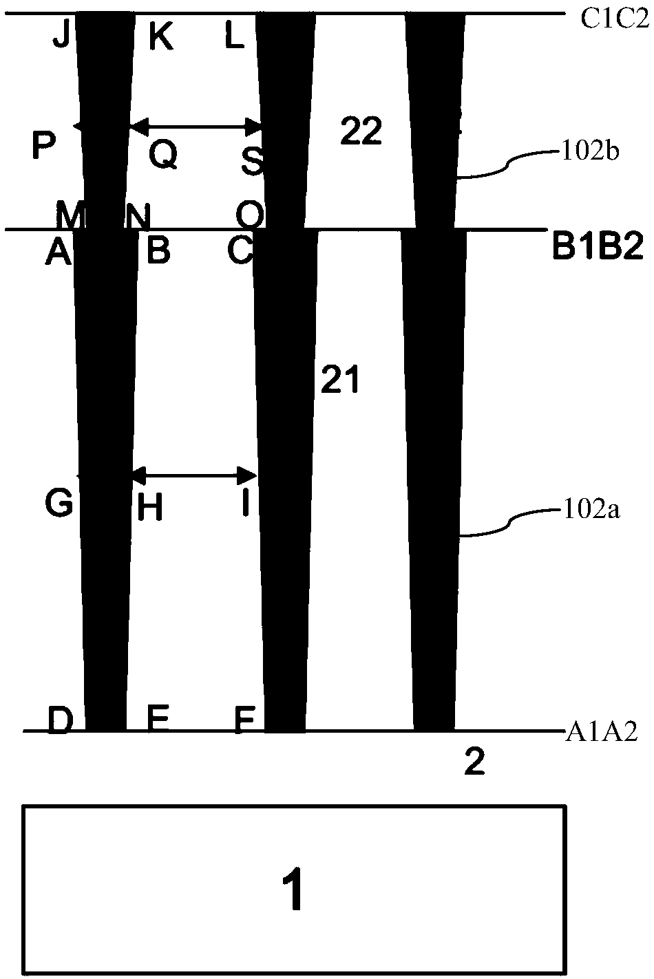
[0056] Such as Figure 1C Shown is the device structure diagram of the super junction structure of the first embodiment of the present invention; figure 2 It is a device structure diagram of a super-junction device formed by adopting the super-junction structure of the first embodiment of the present invention. The super-junction structure of the first embodiment of the present invention includes:

[0057] The first N-type sub-epitaxial layer 2 is formed in the first N-type sub-epitaxial layer 2 with first P-type sub-columns 31 and first N-type sub-columns 21 alternately arranged to form a first super-junction sub-structure.

[0058] The second N-type sub-epitaxial layer is formed on the surface of the first N-type sub-epitaxial layer 2 formed with the first superjunction sub-structure, and the second N-type sub-epitaxial layer is formed in the second N-type sub-epitaxial layer. The seco...

no. 1 example

[0084] for more clarity figure 2 The super junction device of the first embodiment of the present invention is shown, and the device structure of the first embodiment of the present invention will be described below with specific parameters:

[0085] The resistivity of the semiconductor substrate 1 is 0.001 ohm·cm to 0.003 ohm·cm, and the thickness is about 725 microns.

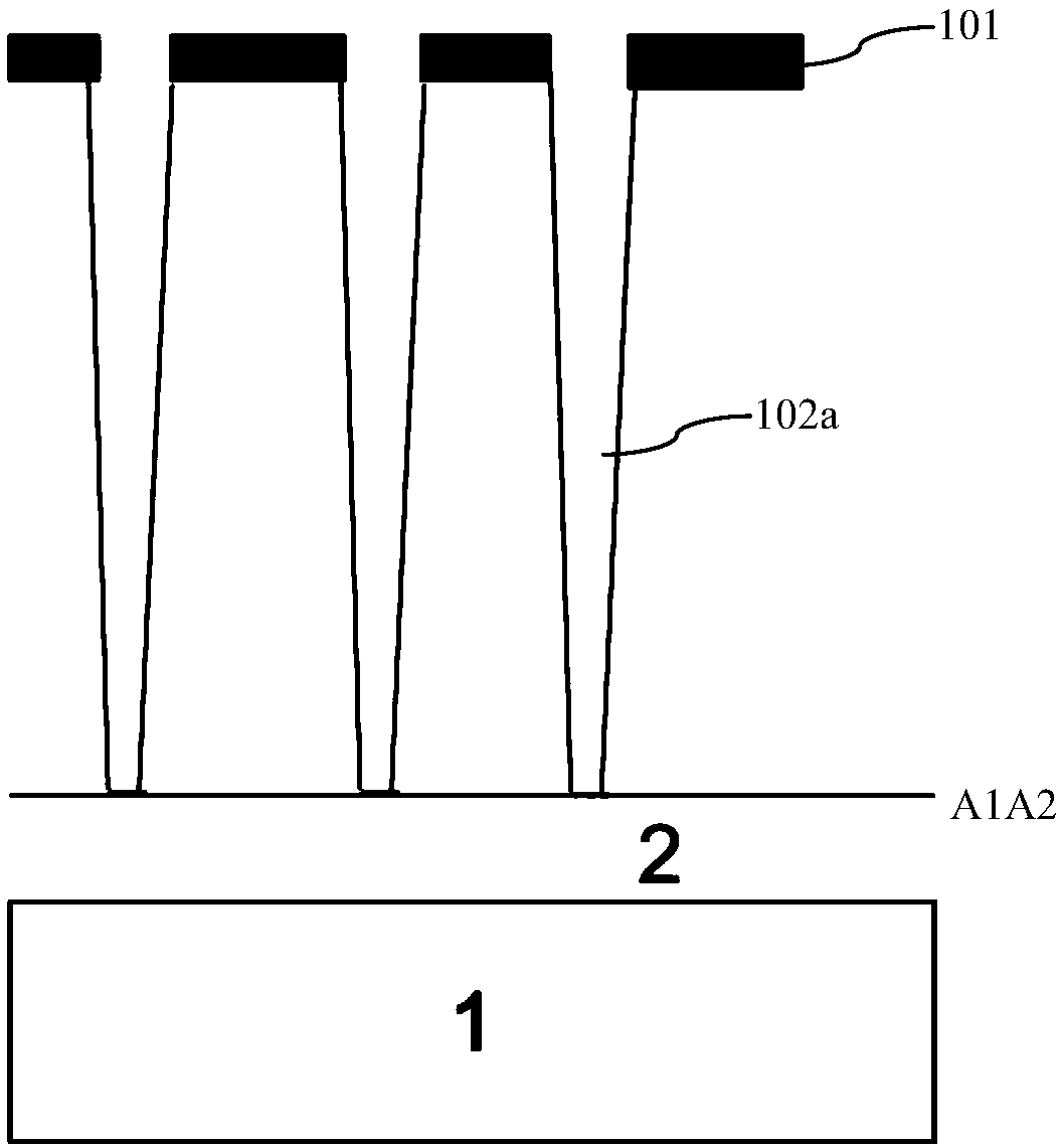
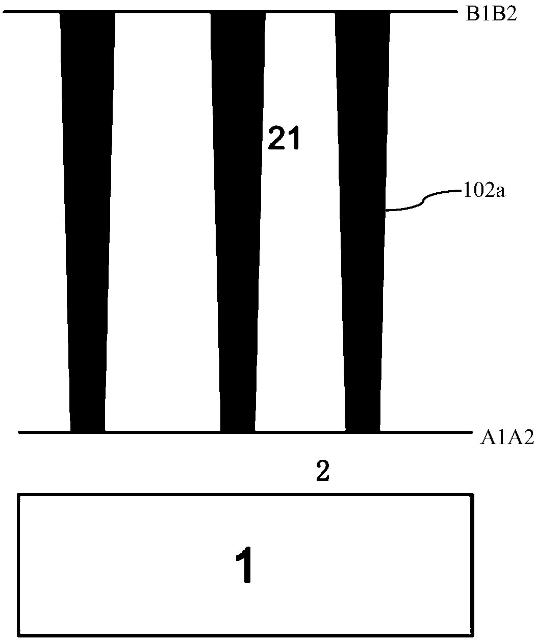
[0086] The position of the bottom surface of the first sub-trench 102a is shown by the line A1A2, and the position of the top surface of the first sub-trench 102a is shown by the line B1B2.

[0087] The first N-type sub-epitaxial layer 2 has a thickness of 45 microns to 50 microns, a resistivity of 1.57 ohm·cm, and a doping concentration of 3.0e15cm -3 The side inclination angle of the first sub-groove 102a is 88.6 degrees, the depth is 40 microns between the line A1A2 and B1B2, the top width is 4 microns, the width AB between the points A and B for short, and the bottom The width between points D and E is...


PUM

PropertyMeasurementUnit
Thicknessaaaaaaaaaa
Thicknessaaaaaaaaaa
Top widthaaaaaaaaaa

Abstract

The invention discloses a super junction structure. The super junction structure is formed by superposing two layers of super junction substructures, each of the two layers of P-type sub-columns consists of a P-type sub-epitaxial layer filled in the corresponding sub-groove; each sub-groove is of a structure with the side face inclined and the top width larger than the bottom width. The top surface is arranged at the position corresponding to the optimal charge balance of the first super junction substructure at the bottom layer plus the change range of plus or minus 5%; the bottom surface isarranged at the position corresponding to the optimal charge balance of the second super junction substructure plus the change range of plus or minus 5%, so the breakdown position of the super junction structure is located at the contact position of the two layers of super junction substructures. The invention further discloses a manufacturing method of the super junction structure. According to the invention, the consistency of device performances such as breakdown voltage and avalanche tolerance can be improved.

Description

technical field [0001] The invention relates to the field of semiconductor integrated circuit manufacturing, in particular to a super junction (super junction) structure; the invention also relates to a manufacturing method of the super junction structure. Background technique [0002] The super junction structure is a structure of alternately arranged N-type pillars and P-type pillars. If the superjunction structure is used to replace the N-type drift region in the vertical double-diffused MOS transistor (Vertical Double-diffused Metal-Oxide-Semiconductor, VDMOS) device, a conduction path is provided in the conduction state. For N-type devices, only N The P-type column provides a path, but the P-type column does not provide it; in the off state, it bears the reverse bias voltage. At this time, the P-type column and the N-type column deplete each other laterally and bear together, forming a super junction metal-oxide semiconductor field effect transistor. (Metal-Oxide-Semic...

Claims


Application Information

Patent Timeline
IPC IPC(8): H01L29/06H01L29/78H01L21/336
CPCH01L29/0634H01L29/7813H01L29/66734
Inventor 肖胜安
Owner SHENZHEN SANRISE TECH CO LTD
Why Eureka
Try Eureka