Etching equipment and crystal edge etching method

A technology of etching equipment and etching gas, which is applied in the manufacture of discharge tubes, electrical components, semiconductors/solid-state devices, etc., can solve problems such as shortening product life, reducing product yield, and damaging wafers, so as to improve service life, The effect of improving product yield and reducing crystal edge defects

Inactive Publication Date: 2019-01-04
HUAIAN IMAGING DEVICE MFGR CORP
View PDF9 Cites 3 Cited by
  • Summary
  • Abstract
  • Description
  • Claims
  • Application Information

AI Technical Summary

Problems solved by technology

However, in the actual manufacturing process, defects will also occur on the back of the wafer. At this time, the defects on the back of the wafer cannot be etched and removed. The defects will evolve into defect sources, gradually forming larger defects, and damaging the wafer. Reduce product yield and shorten product life

Method used


Image

  • Etching equipment and crystal edge etching method
  • Etching equipment and crystal edge etching method
  • Etching equipment and crystal edge etching method

Examples


Embodiment approach 1

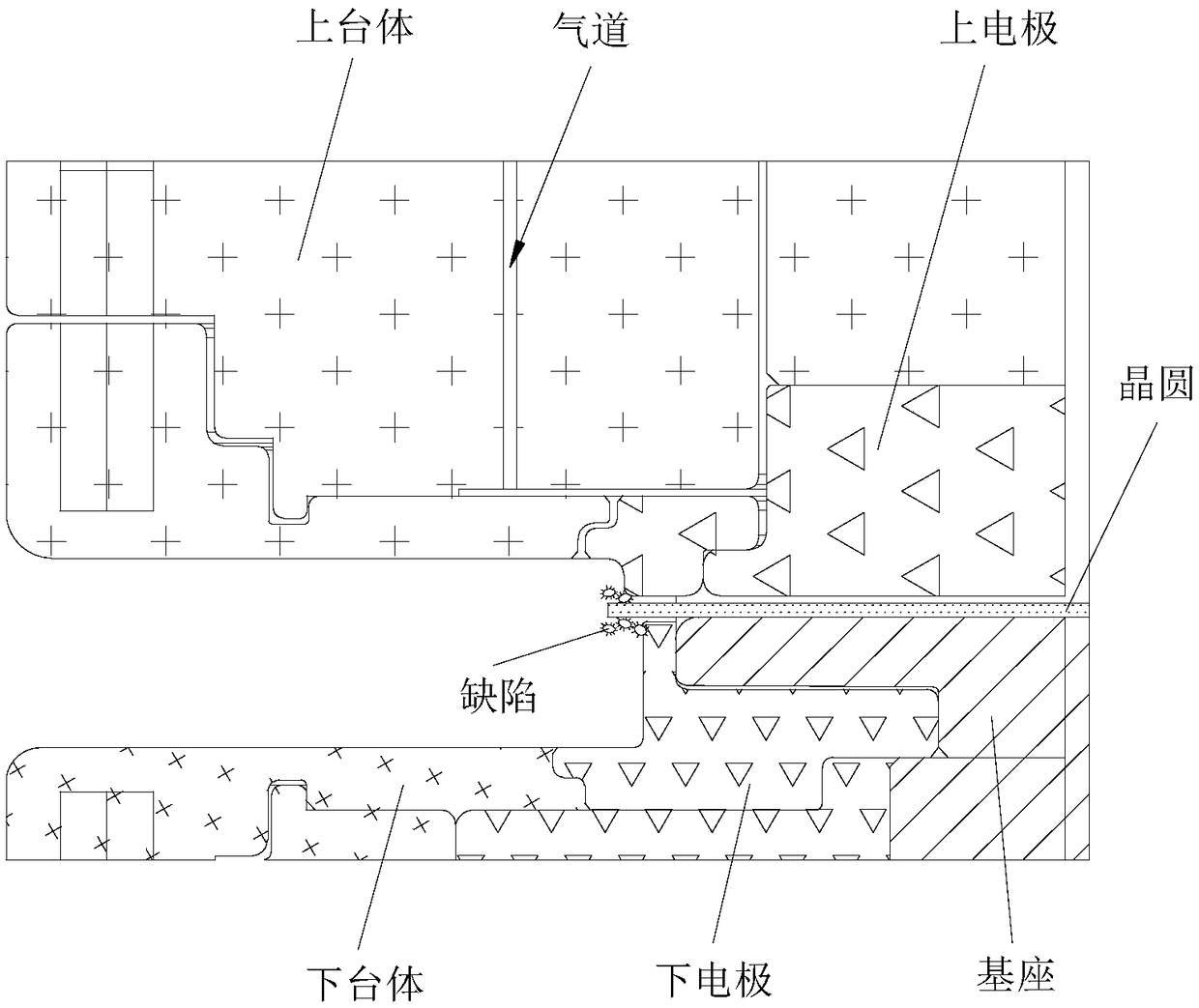
[0053] The first embodiment of the present invention provides an etching device, see figure 2 As shown, it includes an upper platform 1 , a lower platform 2 , an upper electrode 3 and a lower electrode 4 . The upper platform body 1 and the lower platform body 2 are arranged oppositely, and the upper electrode 3 and the lower electrode 4 are correspondingly arranged on the opposite sides of the upper platform body 1 and the lower platform body 2, and the lower electrode 4 is also provided with a substrate for supporting the wafer 6. Seat 5. The etching equipment also includes an etching gas supply assembly 7 , and the upper and lower edges of the wafer 6 are etched by the etching gas supply assembly 7 .

[0054] Using the etching equipment provided by the present invention, when performing edge etching, the wafer 6 is placed on the base 5, and the upper platform 1 drives the upper electrode 3 to move downward, covering and pressing the center of the wafer 6, and engraving Th...

Embodiment approach 2

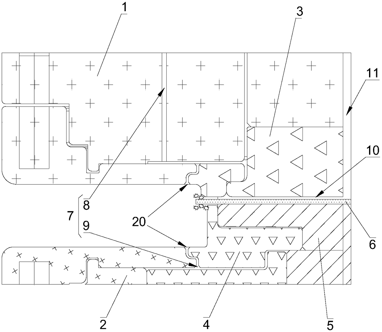
[0067] The second embodiment of the present invention provides an etching device. The main improvement of the second embodiment is that, in the second embodiment of the present invention, the combination image 3 , Figure 4 From the point of view, the etching gas supply assembly 7 includes a main gas source (the main gas source is an external gas source, for simple illustration, not shown in the figure) and a main gas channel 12 communicating with the main gas source. The main gas channel 12 communicates with The etching part 13, when performing edge etching, uses the main gas source to feed the etching gas into the main gas channel 12, and the etching gas reaches the upper and lower edges of the wafer 6 along the main gas channel 12 and through the etching part 13 And etch the upper and lower edges of the wafer 6 . Thereby reducing crystal edge defects and improving product yield.

[0068] In particular, the main gas channel 12 is a channel opened on the upper platform 1, ...

Embodiment approach 3

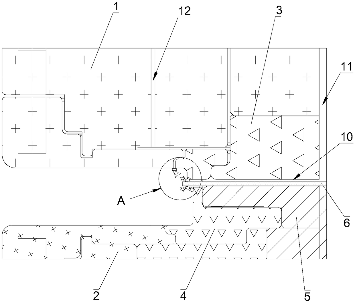
[0075] The third embodiment of the present invention provides an etching device. The main improvement of the third embodiment is that, in the third embodiment of the present invention, the combination Figure 7 with Figure 8From the view, the etching unit 13 includes two second shower heads 18 corresponding to the upper and lower edges of the wafer 6 respectively. When performing edge etching, the etching gas passes through the main gas channel 12 and passes through the two second shower heads 18 to reach the upper and lower edges of the wafer 6 respectively, thereby etching the upper and lower edges of the wafer 6 to reduce edge defects , Improve product yield.

[0076] see Figure 7 As shown, in order to flexibly adjust the injection volume of the etching gas, the etching gas supply assembly 7 further includes a regulating valve 19 . Preferably, the regulating valve 19 is a solenoid valve, and the regulating valve 19 is communicatively connected with the controller 16 . ...


PUM


Abstract

The invention relates to the technical field of semiconductor processing equipment, and discloses etching equipment for removing defects on the back surface of a wafer and a crystal edge etching method. The specific etching equipment includes an upper table body and a lower table body, wherein upper and lower electrodes are respectively arranged on opposite sides of the upper table body and the lower table body, a base for supporting the wafer is arranged on the lower electrode, and the equipment also includes an etching gas supply assembly for etching the upper and lower edges of the wafer. When crystal edge etching is carried out, the wafer is placed on the base, the upper table body drives the upper electrode to move downward, presses and covers the center of the wafer, the etching gassupply assembly introduces gas to the upper and lower edges of the wafer, the defects of the upper and lower edges of the wafer are etched and removed at the same time, and the yield of the product isimproved.

Description

technical field [0001] The invention relates to the technical field of semiconductor processing equipment, in particular to an etching equipment and a crystal edge etching method. Background technique [0002] Etching (Etch) is a very important step in the semiconductor manufacturing process. Etching is associated with photolithography, and the material is patterned. Etching technology is mainly divided into dry etching and wet etching, and dry etching (dryetch) is a technology that uses plasma to etch thin films. When the gas exists in the form of plasma, the chemical activity is much stronger than that under normal conditions. According to the different materials to be etched, choosing a suitable gas can react with the material faster and achieve the purpose of etching and removal. In addition, the electric field is used to guide and accelerate the plasma so that it has a certain amount of energy. When it bombards the surface of the object to be etched, the atoms of the m...

Claims


Application Information

Patent Timeline
Patent Type & Authority Applications(China)
IPC IPC(8): H01J37/32H01L21/3065H01L21/66
CPCH01J37/32449H01J2237/3348H01L21/3065H01L22/26
Inventor 陈峰李天慧黄晓橹
Owner HUAIAN IMAGING DEVICE MFGR CORP
Why Eureka
Try Eureka