Method and system for processing polycrystalline silicon layer before forming of gate insulation layer

A gate insulating layer and polysilicon layer technology, which is applied in the field of polysilicon layer processing methods and processing systems, and can solve problems such as damage and unevenness

Active Publication Date: 2018-07-31
TRULY HUIZHOU SMART DISPLAY
View PDF7 Cites 5 Cited by
  • Summary
  • Abstract
  • Description
  • Claims
  • Application Information

AI Technical Summary

Problems solved by technology

However, DHF will cause some damage to the substrate and P-Si surface, and the

Method used


Image

  • Method and system for processing polycrystalline silicon layer before forming of gate insulation layer
  • Method and system for processing polycrystalline silicon layer before forming of gate insulation layer
  • Method and system for processing polycrystalline silicon layer before forming of gate insulation layer

Examples


Embodiment 1

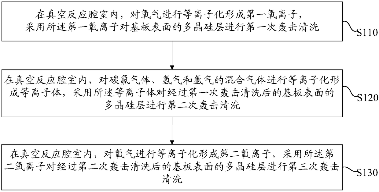
[0053] A polysilicon layer processing method before forming a gate insulating layer, which is applied before forming a gate insulating layer on a polysilicon layer of a substrate, the polysilicon layer processing method includes the following steps:

[0054] In the vacuum reaction chamber, oxygen is plasmatized to form first oxygen ions, and the polysilicon layer on the surface of the substrate is bombarded and cleaned for the first time by using the first oxygen ions; Among them, the flow rate of the oxygen is 1300 sccm, the radio frequency signal source (RF Source) that forms the first oxygen ion is 4000W, the radio frequency bias (RF Bias) is 2000W, and the duration of the first bombardment cleaning is 42 seconds, the pressure of the vacuum reaction chamber is 1Pa;

[0055] In the vacuum reaction chamber, the mixed gas of fluorocarbon gas, hydrogen and argon is plasmaized to form plasma, and the polysilicon layer on the surface of the substrate after the first bombardment c...


PUM


Abstract

The invention discloses a method and system for processing a polycrystalline silicon layer before the forming of a gate insulation layer, and the method comprises the following steps: carrying out theplasma processing of oxygen in a vacuum reaction cavity to form first oxygen ions, and carrying out the first bombardment cleaning of the polycrystalline silicon layer on the surface of a substrate through the first oxygen; carrying out the plasma processing of the mixed gas of fluorocarbon gas, hydrogen gas and argon gas in the vacuum reaction cavity to form plasmas, and carrying out the secondbombardment cleaning of the polycrystalline silicon layer on the surface of the substrate through the plasmas after the first bombardment cleaning; carrying out the plasma processing of the mixed gasof oxygen gas in the vacuum reaction cavity to form second oxygen ions, and carrying out the third bombardment cleaning of the polycrystalline silicon layer on the surface of the substrate through thesecond oxygen ions after the second bombardment cleaning. The method provided by the invention can achieve the removal of the oxides (mainly comprising silicon oxide) on the surface of the polycrystalline silicon layer in a better way, and can reduce mura on a P-Si surface.

Description

technical field [0001] The invention relates to the technical field of display device manufacturing, in particular to a polysilicon layer processing method and processing system before forming a gate insulating layer. Background technique [0002] The interface state between the P-Si layer (polycrystalline silicon) and the GI layer (Gate Insulator, gate insulating layer) in LTPS (Low Temperature Poly-silicon, low temperature polysilicon) is particularly important for the performance of TFT (Thin Film Transistor, thin film transistor). [0003] However, the surface of the P-Si layer is easy to react with air to form a layer of mixture, which is mainly composed of organic matter and oxides. The existence of this mixture makes the interface state between the GI layer and the P-Si layer increase after the GI film is formed. Large, which in turn reduces the mobility of TFT electrons, thereby reducing the performance of TFT. At present, in order to reduce or remove the mixture fo...

Claims


Application Information

Patent Timeline
IPC IPC(8): H01L21/02H01L21/28H01L21/336
CPCH01L21/0206H01L21/28158H01L29/66757
Inventor 刘刚铃木浩司张毅先任思雨苏君海李建华
Owner TRULY HUIZHOU SMART DISPLAY
Why Eureka
Try Eureka