Manufacturing method for gate and semi-conductor device

A manufacturing method and semiconductor technology, applied in the manufacture of semiconductor devices and the field of gate manufacturing, can solve problems affecting the performance of semiconductor devices, affecting the etching of gate layer 14, and reducing production, and achieve strong ability to remove residual defects, The effect of increasing productivity and reducing execution time

Inactive Publication Date: 2009-06-17
SEMICON MFG INT (SHANGHAI) CORP
View PDF1 Cites 5 Cited by
  • Summary
  • Abstract
  • Description
  • Claims
  • Application Information

AI Technical Summary

Problems solved by technology

[0012] However, the method for etching the anti-reflection layer 16 often produces residual defects of the anti-reflection layer material on the surface of the gate layer 14, such as Figure 5 The residue defect shown in 16b
This defect will affect the subsequent etching of

Method used


Image

  • Manufacturing method for gate and semi-conductor device
  • Manufacturing method for gate and semi-conductor device
  • Manufacturing method for gate and semi-conductor device

Examples


Embodiment Construction

[0057] The specific embodiments of the present invention will be described in detail below in conjunction with the accompanying drawings.

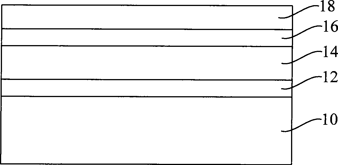
[0058]In an embodiment of the present invention, a method for manufacturing a gate is provided: first, a semiconductor substrate including a gate layer is provided, an anti-reflection layer is formed on the gate layer, and a photolithography layer is formed on the anti-reflection layer. Adhesive layer;

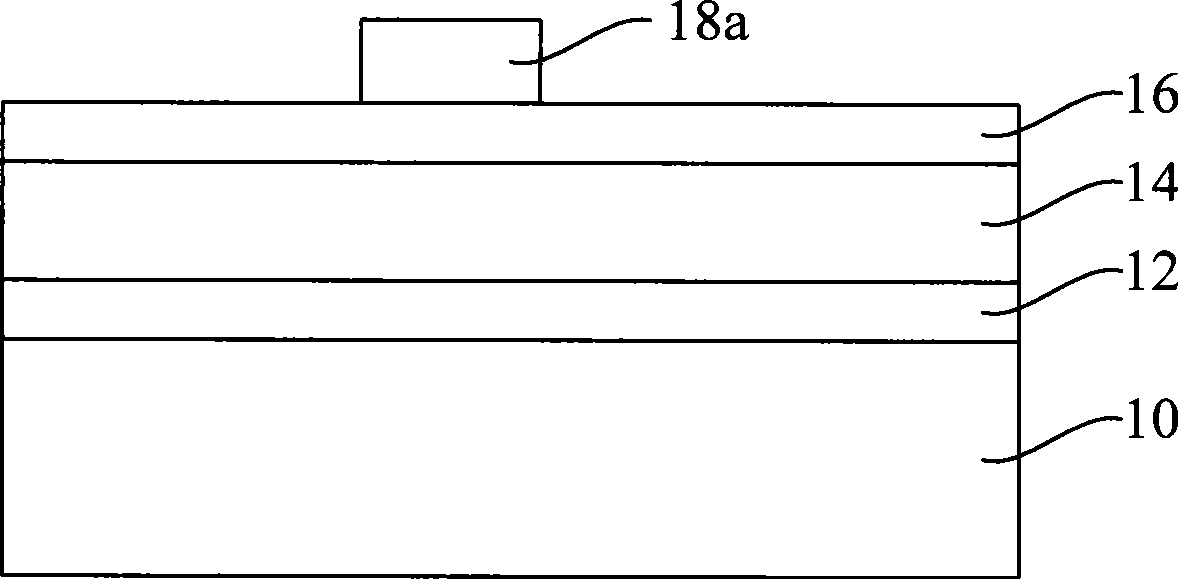
[0059] Next, patterning the photoresist layer to form a photoresist pattern of the gate, the patterning process includes a photolithography process, or a photolithography process and a photoresist reduction process;

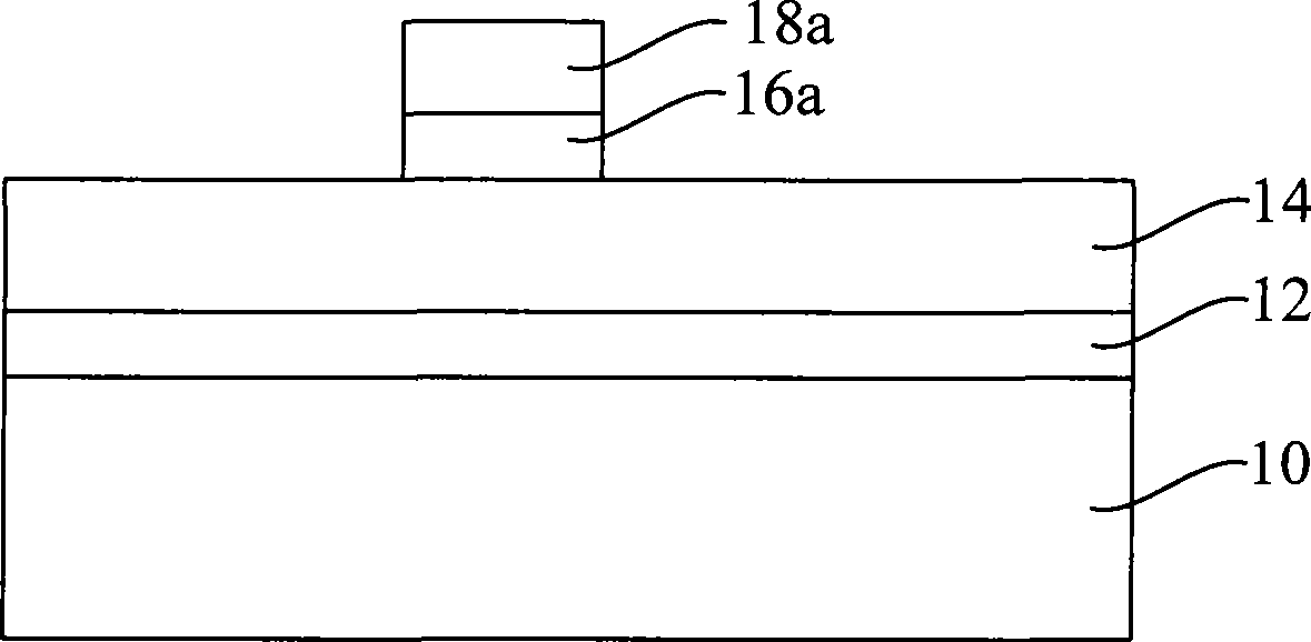
[0060] Then, etching and removing the anti-reflection layer not covered by the photoresist pattern, wherein the etching process includes: performing a main etching process on the anti-reflection layer with plasma; have CF 4 and O 2 performing an over-etching process on the anti-reflection layer with a gas plasma;

[0061]...


PUM


Abstract

A method of manufacturing grids includes steps of sequentially forming a grid layer, an anti-reflection layer and grid photoresist patterns on a semiconductor substrate, etching for removing the anti-reflection layer uncovered by the grid photoresist patterns, etching the grid layer uncovered by the anti-reflection layer, and forming grids, wherein a process of etching the anti-reflection layer includes steps of primarily etching the anti-reflection layer with plasma and over-etching the anti-reflection layer with plasma containing CF4 and O2. The invention further provides a method of manufacturing semiconductor devices. The method of manufacturing grids is capable of reducing residue defects of the anti-reflection layer materials or does not have any residue defects.

Description

technical field [0001] The invention relates to the technical field of semiconductor manufacturing, in particular to a method for manufacturing a gate and a method for manufacturing a semiconductor device. Background technique [0002] With the continuous development of semiconductor integrated circuit manufacturing technology, the line width of semiconductor devices is getting smaller and smaller. At present, the line width of the gate representing the level of photolithography technology has been able to reach 45nm or smaller. A small gate line width can reduce the driving voltage of the formed semiconductor device, thereby reducing power consumption; in addition, it can also reduce the size of the formed semiconductor device, improve the integration level, increase the number of semiconductor devices per unit area, and reduce the power consumption. cost. The Chinese patent application document with the publication number CN 1632921A discloses a gate manufacturing method,...

Claims


Application Information

Patent Timeline
IPC IPC(8): H01L21/28H01L21/311
Inventor 段晓斌黄怡陈海华张海洋
Owner SEMICON MFG INT (SHANGHAI) CORP
Why Eureka
Try Eureka