Self-aligned double patterning method and semiconductor structure formed by same

A double patterning and self-alignment technology, applied in semiconductor/solid-state device manufacturing, electrical components, circuits, etc., can solve problems such as poor reliability and achieve the effect of improving reliability

Pending Publication Date: 2020-08-11
SEMICON MFG INT (SHANGHAI) CORP +1
View PDF3 Cites 7 Cited by
  • Summary
  • Abstract
  • Description
  • Claims
  • Application Information

AI Technical Summary

Problems solved by technology

[0004] However, existing self-aligned dual patterning methods are less reliable

Method used


Image

  • Self-aligned double patterning method and semiconductor structure formed by same
  • Self-aligned double patterning method and semiconductor structure formed by same
  • Self-aligned double patterning method and semiconductor structure formed by same

Examples


Embodiment Construction

[0033] As mentioned in the background, the existing self-aligned double patterning method has poor reliability.

[0034] Figure 1 to Figure 5 It is a structural schematic diagram of each step of a self-aligned double patterning method.

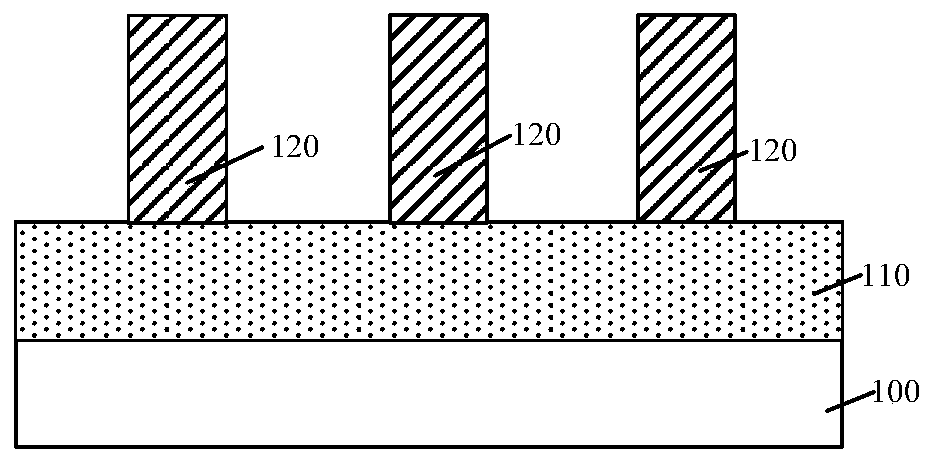
[0035] Please refer to figure 1 A substrate 100 is provided, the surface of the substrate 100 has a material layer 110 to be etched, and several (three are shown in the figure) mutually separated sacrificial layers 120 located on the surface of the material layer 110 to be etched.

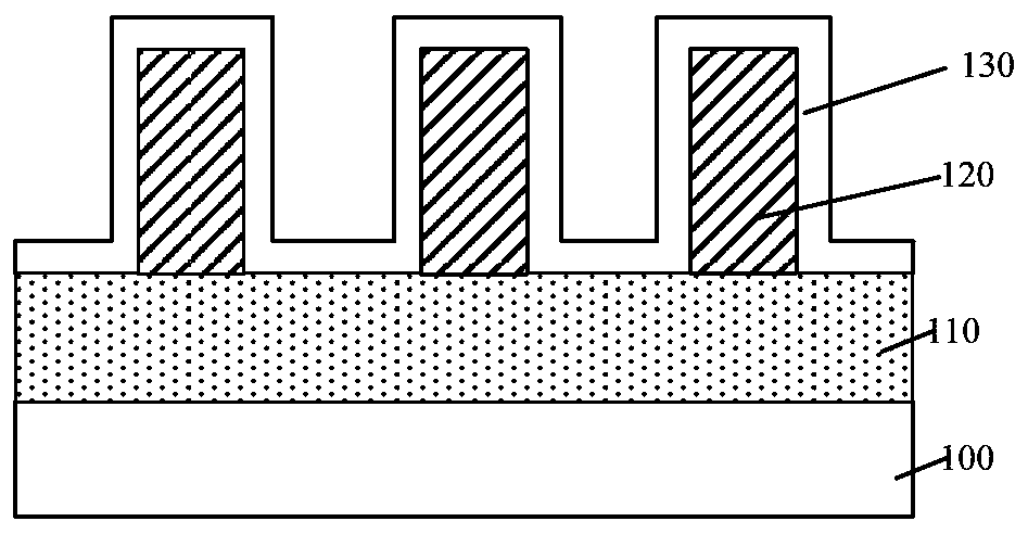
[0036] Please refer to figure 2 , forming a mask material layer 130 on the surface of the material layer 120 to be etched, and the mask material layer 130 covers the top surface and the sidewall surface of the sacrificial layer 120 .

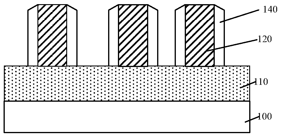
[0037] Please refer to image 3 After the mask material layer 130 is formed, the mask material layer 130 is etched back until the top surface of the sacrificial layer 120 and the top surface of the material layer 110 to be etch...


PUM

PropertyMeasurementUnit
sizeaaaaaaaaaa
sizeaaaaaaaaaa
sizeaaaaaaaaaa

Abstract

The invention relates to a self-aligned double patterning method and a semiconductor structure formed by the same. The method comprises steps of providing a substrate, and enabling a surface of the substrate to be provided with a to-be-etched material layer and a plurality of mutually-separated sacrificial layers located on a surface of the to-be-etched material layer; forming a first mask layer on a surface of a side wall of the sacrificial layer; after the first mask layer is formed, forming a second mask layer on a surface of a side wall of the first mask layer, and the second mask layer and the first mask layer being made of different materials; after the second mask layer is formed, removing the sacrificial layers. The method is advantaged in that reliability of the self-alignment double patterning method is high.

Description

technical field [0001] The invention relates to the technical field of semiconductor manufacturing, in particular to a self-aligned double patterning method and a semiconductor structure formed therefrom. Background technique [0002] With the continuous progress of semiconductor technology, the process nodes of semiconductor devices are continuously reduced. However, due to the limitation of the precision of the existing photolithography process, the mask pattern formed by the existing photolithography process is difficult to meet the demand for continuous reduction of the feature size of semiconductor devices, which hinders the development of semiconductor technology. [0003] In order to further reduce the size of the semiconductor device on the basis of the existing photolithography process, a double patterning process is proposed in the prior art. Among them, especially the self-aligned double patterning (Self-Aligned Double Patterning, SADP) process is widely used bec...

Claims


Application Information

Patent Timeline
Patent Type & Authority Applications(China)
IPC IPC(8): H01L21/033H01L21/02H01L21/311H01L21/67
CPCH01L21/0332H01L21/0337H01L21/0335H01L21/0234H01L21/31116H01L21/67069H01L21/67253
Inventor 刘继全
Owner SEMICON MFG INT (SHANGHAI) CORP
Why Eureka
Try Eureka