Time-of-flight depth camera

A depth camera and time technology, applied in the computer field, can solve the problem of lack of anti-ambient light performance time-of-flight depth camera, etc., to achieve the effect of improving anti-interference ability and reducing power consumption

Pending Publication Date: 2019-02-15
SHENZHEN ORBBEC
0 Cites 41 Cited by

AI-Extracted Technical Summary

Problems solved by technology

[0005] In order to solve the problem of lacking a time-of-flight depth-of-flight camera with good anti-environm...

Method used

In one embodiment, the light source 303 is a laser light source, and its surface of the MEMS scanner 305 includes a blazed grating, so that stripes can be generated in a predetermined direction, and a denser fringe pattern can be produced by scanning the MEMS scanner 305 , thereby improving the resolution of the depth image.
[0032] In some embodiments, the spatial light modulator 113 is also used to expand the received carrier light beam to expand the field of view.
[0036] The light source 201 can be a single light source or an array of light sources. In one embodiment, the light source 201 is a light source array composed of a plurality of regular light sources, such as a VCSEL array chip composed of a semiconductor substrate and a plurality of VCSEL light sources arranged on the substrate. The DOE204 replicates the arrayed beams emitted by the light source 201, and the non-flooded beams emitted outward are composed of multiple replicated arrayed beams, thereby expanding the field of view and the number of beams.
[0039] FIG. 3 is a schematic diagram of a launch module according to yet another embodiment of the present invention. The emission module 11 includes a light source 303, a drive circuit 304, a beam scanner 305, and may also include a lens unit (not shown in the figure). The light beam emitted by the light source 303 is reflected/diffraction by the beam scanner 305 and then emitte...

Abstract

The invention provides a time-of-flight depth camera, which includes a transmitting module used for transmitting a light beam, a collecting module used for collecting a reflected light beam, and a processing circuit connected with the transmitting module and the collecting module and used for calculating the time of flight between the transmitted light beam and the reflected light beam. The transmitting module includes a light source, a time light modulator and a space light modulator. The time light modulator is used for making the light source emit corresponding carrier beams with one time carrier signal. The space light modulator is used for modulating the carrier beams spatially to form non-flooding carrier beams and emitting the non-flooding carrier beams outward. The collecting module includes an array pixel unit and a lens unit. The lens unit is used for receiving and imaging at least part of the non-flooding carrier beams reflected by an object on at least part of the array pixel unit. Non-flooding carrier beams are formed through modulation of the light source by the time light modulator and the space light modulator, so as to enhance the anti-interference ability of the time-of-flight depth camera to ambient light and reduce power consumption.

Application Domain

Electromagnetic wave reradiation

Technology Topic

Carrier signalLight source +5

Image

  • Time-of-flight depth camera
  • Time-of-flight depth camera
  • Time-of-flight depth camera

Examples

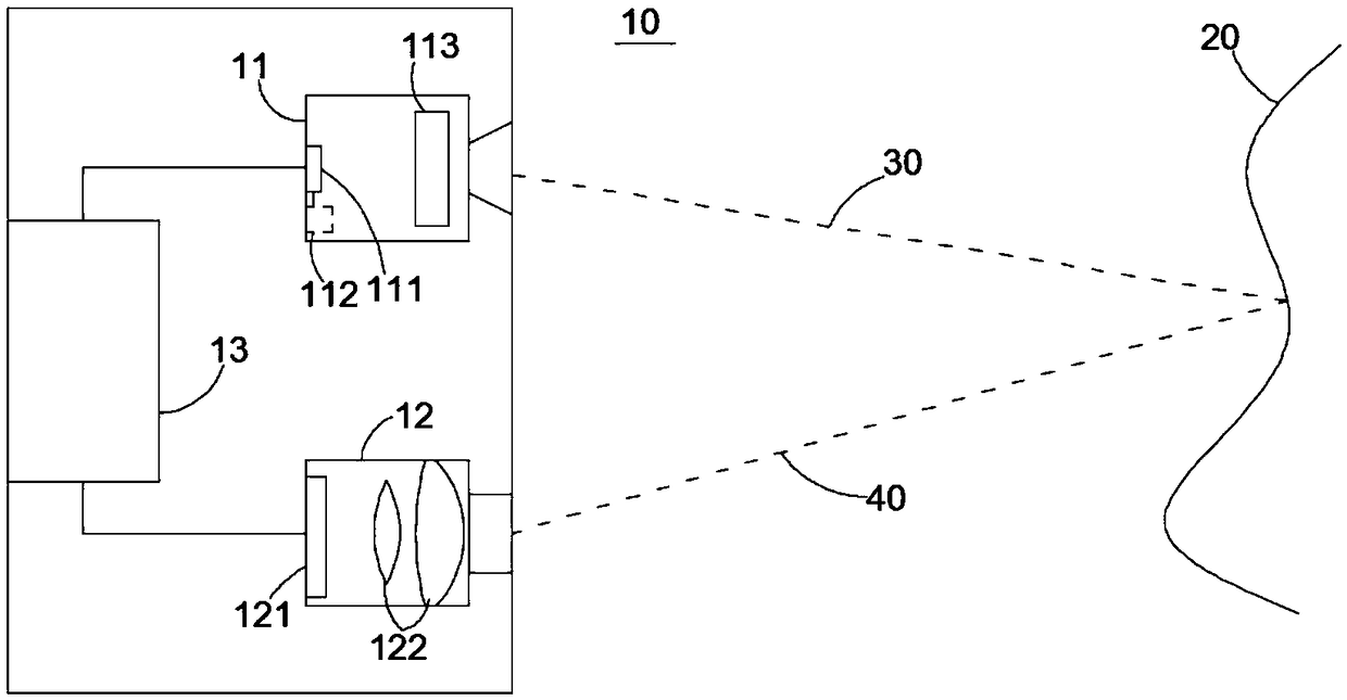
  • Experimental program(1)

Example Embodiment

[0021] In order to make the technical problems, technical solutions and beneficial effects to be solved by the embodiments of the present invention clearer, the present invention will be further described in detail below with reference to the accompanying drawings and embodiments. It should be understood that the specific embodiments described herein are only used to explain the present invention, but not to limit the present invention.
[0022] It should be noted that when an element is referred to as being "fixed to" or "disposed on" another element, it can be directly on the other element or indirectly on the other element. When an element is referred to as being "connected to" another element, it can be directly connected to the other element or indirectly connected to the other element. In addition, the connection can be used for either a fixing function or a circuit connecting function.
[0023] It is to be understood that the terms "length", "width", "upper", "lower", "front", "rear", "left", "right", "vertical", "horizontal", "top" , "bottom", "inside", "outside", etc. indicate the orientation or positional relationship based on the orientation or positional relationship shown in the accompanying drawings, which are only for the convenience of describing the embodiments of the present invention and simplifying the description, rather than indicating or implying that The device or element must have a specific orientation, be constructed and operated in a specific orientation, and therefore should not be construed as a limitation of the present invention.
[0024] In addition, the terms "first" and "second" are only used for descriptive purposes, and should not be construed as indicating or implying relative importance or implying the number of indicated technical features. Thus, a feature defined as "first", "second" may expressly or implicitly include one or more of that feature. In the description of the embodiments of the present invention, "plurality" means two or more, unless otherwise expressly and specifically defined.
[0025] The present invention provides a time-of-flight depth camera, which has strong resistance to ambient light. It can be understood that this solution can not only solve the problem of ambient light interference, but also solve other problems, such as the problem of high power consumption, etc. .
[0026] figure 1 is a schematic diagram of a time-of-flight depth camera according to an embodiment of the present invention. The time-of-flight depth camera 10 includes an emission module 11 , an acquisition module 12 and a processing circuit 13 , wherein the emission module 11 provides an emission beam 30 to the target space to illuminate the object 20 in the space, and at least part of the emission beam 30 is reflected by the object 20 Then, a reflected beam 40 is formed, and at least part of the reflected beam 40 is collected by the acquisition module 12. The processing circuit 13 is connected to the transmitter module 11 and the acquisition module 12 respectively, and the trigger signals of the transmitter module 11 and the acquisition module 12 are synchronized to calculate The time required for the light beam to be emitted by the emission module 11 and received by the acquisition module 12 is the time-of-flight t between the emission light beam 30 and the reflected light beam 40, and further, the distance D of the corresponding point on the object can be calculated by the following formula:
[0027] D=c·t/2 (1)
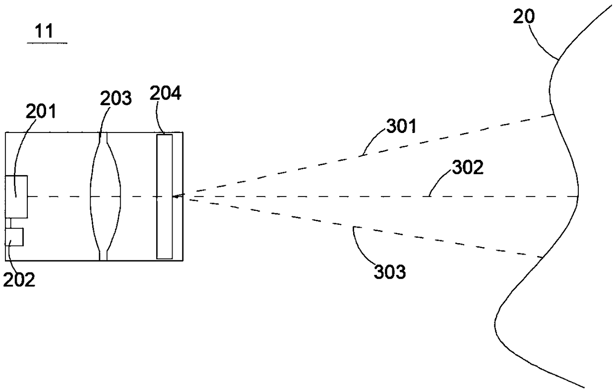
[0028] where c is the speed of light.
[0029] The emission module 11 includes a light source 111 , a temporal light modulator 112 and a spatial light modulator 113 . The light source 111 can be a light source such as a light emitting diode (LED), an edge emitting laser (EEL), a vertical cavity surface emitting laser (VCSEL), etc., or a light source array composed of multiple light sources, and the light beam emitted by the light source can be visible light, infrared light , UV light, etc.
[0030] The time light modulator 112 provides a time carrier signal to the light source 111 to control the light source 111 to emit a corresponding carrier beam. For example, in one embodiment, the carrier signal is a pulsed signal with a certain frequency, and the light source 111 emits a pulsed beam at this frequency, which can be used in direct time-of-flight (DirectTOF) measurement; in one embodiment, the carrier signal is a pulsed signal with a certain frequency. A square wave signal or a sine signal of a certain wavelength, the amplitude of the light source 111 is modulated by the carrier signal to emit a corresponding square wave beam or a sine wave beam, which can be used in indirect time-of-flight (Indirect TOF) measurement. It can be understood that the temporal light modulator 112 may be an independent control circuit or a processing circuit 13 , for example, the processing circuit 13 implements carrier modulation on the amplitude of the light source by modulating the power of the light source. The frequency of the carrier signal is set according to the measurement distance, for example, it can be set to 1MHz to 100MHz, and the measurement distance is from several meters to several hundreds of meters.
[0031] The spatial light modulator 113 receives the carrier beam from the light source 111, and spatially modulates the carrier beam, that is, modulates the distribution of the carrier beam in space to form a non-flooding carrier beam with uneven intensity distribution to be emitted outward. Compared with the traditional flood light beam, due to the uneven intensity distribution of the non-flood light beam, under the same light source power, the area with higher intensity distribution will have higher anti-interference performance to ambient light; When the field of view is the same, due to the non-uniformity of the intensity distribution, to achieve the same anti-interference performance of ambient light, flood lighting requires higher power consumption.
[0032] In some embodiments, the spatial light modulator 113 is also used to expand the received carrier beam to expand the field of view.
[0033] The processing circuit 13 may be an independent dedicated circuit, such as a dedicated SOC chip, FPGA chip, ASIC chip, etc., or may include a general-purpose processor, for example, when the depth camera is integrated into a smart terminal such as a mobile phone, a TV, a computer, etc., A processor in the terminal can be used as at least a part of the processing circuit 13 .
[0034] In some embodiments, the time-of-flight depth camera 10 may further include a color camera, an infrared camera, an IMU and other devices, and the combination with these devices can realize more abundant functions, such as 3D texture modeling, infrared face recognition, SLAM and other functions .
[0035] figure 2It is a schematic diagram of a launch module according to an embodiment of the present invention. The emission module 11 includes a light source 201 , a driving circuit 202 , a lens 203 and a diffractive optical element (DOE) 204 . The light source 201 emits a pulse, square wave or sine wave modulated light beam under the power time modulation of the driving circuit 202 , and the light beam passes through the lens 203 After being collimated or focused, it is incident on the DOE204, and the DOE204 performs spatial modulation on the incident beam, that is, diffraction. In one embodiment, the DOE 204 splits the incident beam and emits a plurality of beams 301 , 302 and 303 into the target space, such as tens of thousands of beams, each beam forming a spot on the surface of the object 20 . In one embodiment, the DOE 204 will form a regular array of spots by diffracting the incident beam (meaning that the angular offset of each spot is uniformly distributed, and the regular array is incident on the surface of the 3D object, and the array will be reconstructed). In one embodiment, the DOE 204 will form a speckle pattern by diffracting the incident light beam, that is, the speckle arrangement has a certain randomness.
[0036] The light source 201 may be a single light source or an array of light sources. In one embodiment, the light source 201 is a light source array composed of a plurality of regular light sources, such as a VCSEL array chip composed of a semiconductor substrate and a plurality of VCSEL light sources arranged on the substrate. The DOE 204 replicates the array beam emitted by the light source 201, and the non-flood beam emitted outward is composed of a plurality of replicated array beams, thereby expanding the field of view and the number of beams.
[0037] In some embodiments, the spatial light modulator in the emission module 11 may also include a mask, and the mask includes a two-dimensional pattern for modulating the incident light beam into a non-flood light beam. The beam is spatially modulated to form a two-dimensional encoded pattern beam.
[0038] In some embodiments, the spatial light modulator in the emission module 11 may also include a microlens array, and the microlens array is formed by arranging a plurality of microlens units. After the light beam of 201, an array light beam corresponding to the arrangement of the microlens units is generated and emitted outward; in one embodiment, the light source 201 also includes a plurality of sub-light sources corresponding to the arrangement in the microlens array, and each microlens unit receives the corresponding sub-light sources. The beams of the sub-light sources are collimated or focused and then the array beams are emitted outward. The array beams can be in a random arrangement or a regular arrangement.
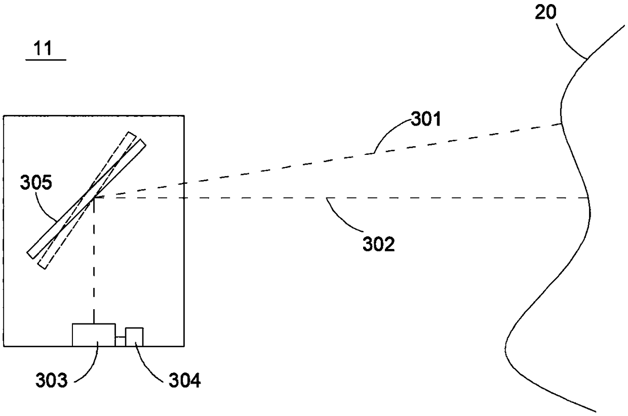
[0039] image 3 It is a schematic diagram of a transmitting module according to another embodiment of the present invention. The emission module 11 includes a light source 303, a driving circuit 304, a beam scanner 305, and may also include a lens unit (not shown in the figure). The light beam emitted by the light source 303 is reflected/diffracted by the beam scanner 305 and then emitted to the target space. The driving circuit 304 performs sequential power modulation on the light source 201 to emit a pulsed, square wave or sine wave modulated beam, and the beam scanner 305 rotates along a single axis or multiple axes to emit the beam into the target space. In one embodiment, the beam scanner includes a micro-electromechanical system (MEMS) scanner. Due to the extremely high scanning frequency and the small volume, the emission module can have a small volume and high performance. The MEMS scanner can scan at a frequency of 1MHz to 20MHz, so it can provide sufficient spatial and temporal resolution. Through the configuration of the driving circuit 304 and the beam scanner 305, the beam emitted by the light source 303 can be spatially and temporally modulated to produce various patterns of beam output, such as regular spot patterns, fringe patterns, and sinusoidal spatial patterns.
[0040] In one embodiment, the light source 303 is a laser light source, and the surface of the MEMS scanner 305 includes a blazed grating, so that fringes can be generated in a predetermined direction, and a denser fringe pattern can be generated by scanning the MEMS scanner 305, thereby The resolution of the depth image can be increased.
[0041] In some embodiments, the beam scanner 305 may also be a liquid crystal light modulator, a nanochip modulator, or the like.
[0042] back figure 1 The acquisition module 12 includes an array pixel unit 121 and a lens unit 122. The lens unit 122 receives and images at least part of the non-flood carrier beam reflected from the object on at least part of the array pixel unit 121. The array pixel unit 121 may be an array pixel unit composed of a charge coupled element (CCD), a complementary metal oxide semiconductor (CMOS), an avalanche diode (AD), a single photon avalanche diode (SPAD), etc. The size of the array represents the depth of the camera. Resolution, such as 320x240, etc. Generally, connected to the array pixel unit 121 also includes a readout circuit (not shown in the figure) composed of one or more of a signal amplifier, a time-to-digital converter (TDC), an analog-to-digital converter (ADC) and other devices. out).
[0043] Figure 4 It is a schematic diagram of an array pixel unit according to an embodiment of the present invention. The array pixel unit 40 includes a plurality of pixel units 401 for receiving the light beams reflected back by the object, and converting the light energy or the number of photons into electrical signals for output by the readout circuit 50 . In this embodiment, it is assumed that what is reflected by the object is a speckle pattern composed of a plurality of spots 60. By setting the lens, the emission module, etc., the spots can be configured to an appropriate size for imaging on the array pixel unit. superior. For example, in this embodiment, the size of the spot occupies about 4 pixel areas. It can be understood that the size of the spot can also be set to a single pixel, two pixels or other number of pixel areas, so that the array pixel unit 40 is divided into a plurality of sub-pixel unit areas according to the incident light beam.
[0044] In this embodiment, it is assumed that a single speckle is imaged on a sub-pixel unit consisting of four pixels A, B, C, and D, and the speckle amplitude in the speckle pattern is modulated by a sine wave or a square wave, and the modulation period is T. The four pixels A, B, C, and D are set to be activated at different times within a single cycle time, such as 0~T/2, T/2~T, T/4~3T/4, 3T/4~ It is activated for 5T/4 time to collect the light beam, and the optical signal values ​​I1, I2, I3 and I4 are obtained respectively. Since the four pixels correspond to the same spot, when the spot is small enough, the object corresponding to the spot can be regarded as a spot, that is, the depth values ​​on the four pixels are considered to be the same. Based on this, the processing circuit can use the four-step phase shift method. , the distance value (including the flight time) of the spots on the four pixels A, B, C, and D will be calculated by the following formula:
[0045] D=C·T·atan2(I1-I3,I4-I2)/(4·π) (2)
[0046] It can be understood that for multi-step phase shifting, the size of the spots can be adjusted accordingly.
[0047] In some embodiments, the blobs are configured to be 2 pixel units in size, such as ellipses. The spot amplitude is modulated by pulse, the pulse period is T, one of the 2 pixel units is activated in synchronization with the pulse of the transmitter module, and receives the beam within 0~T/2 time, and the other receives the beam within T/2~T time The light beams generate electrical signals I1 and I2, respectively. Then the depth value (including the flight time) of the target object corresponding to the two pixels can be calculated by the following formula:
[0048]
[0049] In some embodiments, the blobs are configured to be at least 3 or more pixel units in size. The spot amplitude is modulated by pulses, and the pulse period is T. At least 3 of the multiple pixel units collect the background light signal I0 within the time of 0~T/3 respectively, collect the light signal I1 at the time of T/3~2T/3, and collect the light signal I1 at the time of 2T. /3~T collects the optical signal I2. Or collect the optical signal I1 within 0~T/3, collect the light signal I2 at T/3~2T/3, collect the background light signal I0 at 2T/3~T, and then calculate the distance value of the target object.
[0050]
[0051] The above is just to better illustrate how to use the speckle pattern for distance calculation, and several possible modulation and distance depth calculation methods are listed. Other possible modulation methods and distance calculation formulas are also applicable to our proposed non-flooding pattern. .
[0052] In order to increase the resolution of the depth image, in some embodiments, the distance between adjacent spots should not be too large. Preferably, the distance between adjacent spots along a certain direction is set to not exceed the size of the spot itself along the direction. For example, the lateral size of the spot is M, and the interval between adjacent spots along the lateral direction is N, then N
[0053] Compared with the traditional single-pixel calculation, the calculation efficiency is greatly improved by performing timing control on multiple pixels that fall into the same spot and approximately calculating the depth value. Moreover, compared with the floodlight pattern, since the range of a single spot is smaller, multiple pixels falling into a single spot can be identified (the floodlight pattern cannot be located in multiple pixels with the same phase), and the calculated depth value More credibility.
[0054] It can be understood that, in the above embodiments, the non-flood light carrier beam formed by the spots is used as an example for description, and the above solution is also applicable to other non-flood light carrier light beams, such as stripes and two-dimensional coding patterns.
[0055] Figure 5 It is a schematic diagram of steps of a method for calculating flight time according to an embodiment of the present application. The time-of-flight calculation method is based on the above-mentioned time-of-flight depth camera, and is executed in the form of a processing circuit, software, a combination of software and hardware, and the like. In step 511, the non-flood carrier beam is emitted outward by the emission module, and the emission module is such as figure 2 , image 3 And as shown in each of the above-mentioned embodiments, the emitted non-flooding carrier beams include speckle, regular spots, two-dimensional codes, stripes and other non-flooding forms of carrier beams; in step 512, the collection module is used to collect objects At least part of the reflected non-flood carrier beam, after the emission module emits the beam, illuminates the object in the target space, and is reflected by the object, and at least part of the reflected non-flood carrier beam is received by the acquisition module , the acquisition module such as Figure 4 and shown in the above-mentioned embodiments; in step 513, the time-of-flight between the emission and reflection of the non-flooding carrier beam is calculated, that is, the non-flooding carrier beam is recorded and calculated by the processing circuit through phase, high-speed shutter, etc. The time-of-flight between the beam and the reflected beam, the specific calculation method is described in the previous description, such as the 2-phase, 3-phase and 4-phase calculation methods.
[0056] The above content is a further detailed description of the present invention in combination with specific preferred embodiments, and it cannot be considered that the specific implementation of the present invention is limited to these descriptions. For those skilled in the art to which the present invention belongs, under the premise of not departing from the concept of the present invention, several equivalent substitutions or obvious modifications can be made, and the performance or use is the same, which should be regarded as belonging to the protection scope of the present invention.

PUM

no PUM

Description & Claims & Application Information

We can also present the details of the Description, Claims and Application information to help users get a comprehensive understanding of the technical details of the patent, such as background art, summary of invention, brief description of drawings, description of embodiments, and other original content. On the other hand, users can also determine the specific scope of protection of the technology through the list of claims; as well as understand the changes in the life cycle of the technology with the presentation of the patent timeline. Login to view more.

Similar technology patents

Data sending and receiving methods based on LoRa

ActiveCN108494527AImprove anti-interference abilityImprove transmission reliability
Owner:TSINGHUA UNIV

Low-loss metamaterial antenna housing

InactiveCN103296402AEnhanced wave performanceImprove anti-interference ability
Owner:KUANG CHI INNOVATIVE TECH

Classification and recommendation of technical efficacy words

  • Improve anti-interference ability
  • reduce power consumption

Composite electromagnetic shielding paint based on nano carbon material

InactiveCN105331264AImprove anti-interference abilityGood protection against electromagnetic radiation
Owner:INST OF URBAN ENVIRONMENT CHINESE ACAD OF SCI

Brushless direct current motor electronic speed governor based on STM32

InactiveCN103051262AImprove real-time and stabilityImprove anti-interference ability
Owner:GUANGXI NORMAL UNIV

Electrode array for use in medical stimulation and methods thereof

InactiveUS20050038489A1reduce power consumptionincrease battery life
Owner:CASE WESTERN RESERVE UNIV

Method of reselecting a cell based on priorities

ActiveUS20090181676A1ensure quality of servicereduce power consumption
Owner:LG ELECTRONICS INC

Organic light-emitting devices with mixed electron transport materials

InactiveUS20060204784A1good luminance efficiency and stabilityreduce power consumption
Owner:EASTMAN KODAK CO
Why Eureka
Try Eureka