Array substrate and preparation method thereof

A technology for array substrates and substrate substrates, which is applied in the field of array substrates and their preparation, and can solve problems such as prone to short circuits and decreased panel yields

Active Publication Date: 2019-02-22
HEFEI XINSHENG OPTOELECTRONICS TECH CO LTD +1
View PDF14 Cites 3 Cited by
  • Summary
  • Abstract
  • Description
  • Claims
  • Application Information

AI Technical Summary

Problems solved by technology

[0003] The main purpose of the present invention is to provide an array substrate and its preparation method, which is used to solve the problem ...

Method used


Image

  • Array substrate and preparation method thereof
  • Array substrate and preparation method thereof
  • Array substrate and preparation method thereof

Examples


Embodiment Construction

[0036] The following will clearly and completely describe the technical solutions in the embodiments of the present invention with reference to the accompanying drawings in the embodiments of the present invention. Obviously, the described embodiments are only some, not all, embodiments of the present invention. Based on the embodiments of the present invention, all other embodiments obtained by persons of ordinary skill in the art without making creative efforts belong to the protection scope of the present invention.

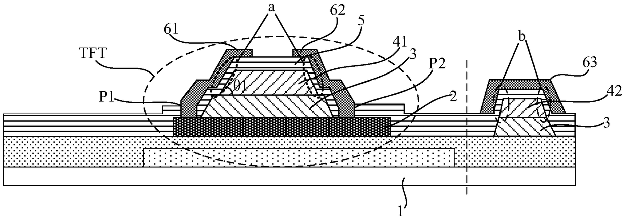
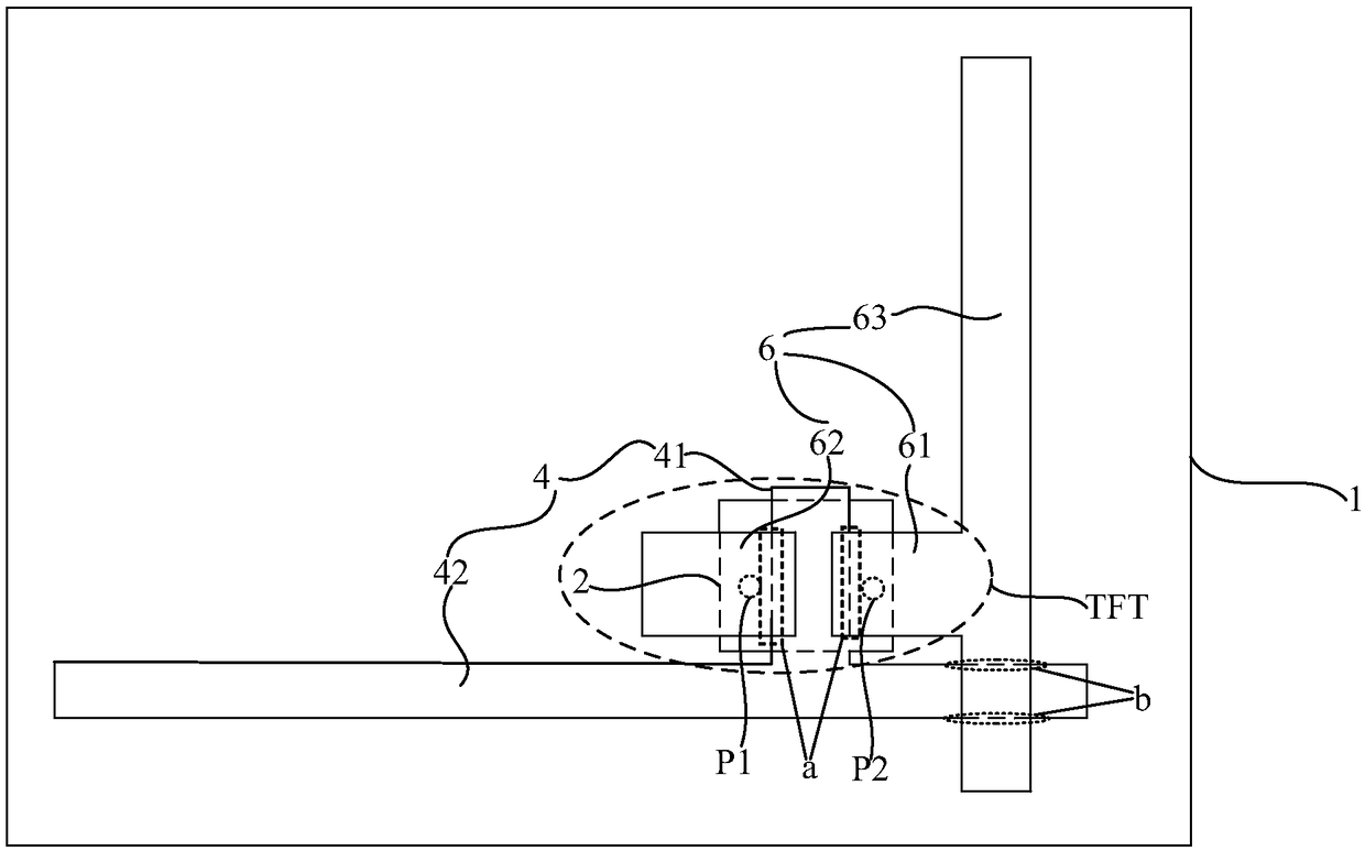
[0037] The TFT (Thin Film Transistor, Thin Film Transistor) of the top-gate structure has attracted attention because of its higher on-state current, higher aperture ratio and better TFT stability than the TFT of the bottom-gate structure.

[0038] like figure 1 and figure 2 As shown, the array substrate of a TFT with a top-gate structure in the related art includes a base substrate 1, and an active layer 2, a gate insulating layer 3, a gate metal layer 4, a...


PUM


Abstract

The invention relates to the technical field of display, especially to an array substrate and a preparation method thereof. The array substrate and the preparation method thereof are used to solve theproblem that overlap regions between a gate and a source and a drain are prone to short circuit in the related art, which causes the decrease of panel yield. The embodiments of the invention providesthe array substrate. Multiple TFTs are arranged on the array substrate. Each TFT includes an active layer, a gate insulating layer, a gate, a first interlayer insulating layer, a second interlayer insulating layer, a source and a drain which are arranged on the substrate in order. Each source and drain are in contact with the corresponding active layer at least passing through a hole through thecorresponding first interlayer insulating layer. Each second interlayer insulating layer includes a first insulation pattern. Each first insulation pattern is located between the corresponding first interlayer insulating layer and the corresponding source and the corresponding drain and is located in the area where the corresponding TFT is located. Each first insulation pattern at least covers anoverlap region between the corresponding source and the corresponding drain and the side surface of the corresponding gate in the area where the corresponding TFT is located. The array substrate and the preparation method thereof are used for production and manufacturing of display panels.

Description

technical field [0001] The present invention relates to the field of display technology, in particular to an array substrate and a preparation method thereof. Background technique [0002] Currently, a thin film transistor (Thin Film Transistor, TFT) is a main driving element of a liquid crystal display and an active matrix organic light emitting diode (Active Matrix Organic Light Emitting Diode, AMOLED). Contents of the invention [0003] The main purpose of the present invention is to provide an array substrate and its preparation method, which is used to solve the problem in the related art that the overlapping area between the gate, the source and the drain is prone to short circuit, resulting in a decrease in panel yield. [0004] To achieve the above object, the present invention adopts the following technical solutions: [0005] In a first aspect, an embodiment of the present invention provides an array substrate, including a base substrate and a plurality of TFTs ...

Claims


Application Information

Patent Timeline
IPC IPC(8): H01L27/12H01L29/786H01L21/77
CPCH01L27/1237H01L27/124H01L27/1259H01L29/78618H01L29/78633
Inventor 刘军闫梁臣周斌方金钢李广耀苏同上罗标桂学海
Owner HEFEI XINSHENG OPTOELECTRONICS TECH CO LTD
Why Eureka
Try Eureka