Method for Detecting Missing Defects in Embedded SiGe Epitaxy

An embedded silicon germanium and silicon germanium epitaxy technology, which is applied in semiconductor/solid-state device testing/measurement, electrical components, circuits, etc., can solve the problems of CMOS device yield decline, time-consuming, and inability to observe defects, etc.

Active Publication Date: 2018-05-11
SHANGHAI HUALI INTEGRATED CIRCUTE MFG CO LTD
View PDF4 Cites 0 Cited by
  • Summary
  • Abstract
  • Description
  • Claims
  • Application Information

AI Technical Summary

Problems solved by technology

Missing defects in SiGe can lead to severe electrical leakage, causing complete failure of the device and resulting in a decrease in the yield of CMOS devices
[0005] The current method of detecting silicon germanium epitaxial defects is to use the principle of optical reflection to measure the points with different surface roughness on the silicon wafer, but this method cannot distinguish the difference between the actual defect and the surface roughness, and because the actual defect size has been compared with the surface roughness Similarly, most of the measured results are rough surfaces, which cannot effectively observe defects
Another method is to use TEM (transmission electron microscope) to analyze the grown SiGe (silicon germanium) film, but because the sample size analyzed by TEM is very small, the probability of relatively catching defects is also very small, and it is too time-consuming. It is not conducive to shortening the R&D cycle, and it is difficult to provide effective reference value for online process window optimization

Method used


Image

  • Method for Detecting Missing Defects in Embedded SiGe Epitaxy
  • Method for Detecting Missing Defects in Embedded SiGe Epitaxy
  • Method for Detecting Missing Defects in Embedded SiGe Epitaxy

Examples


Embodiment Construction

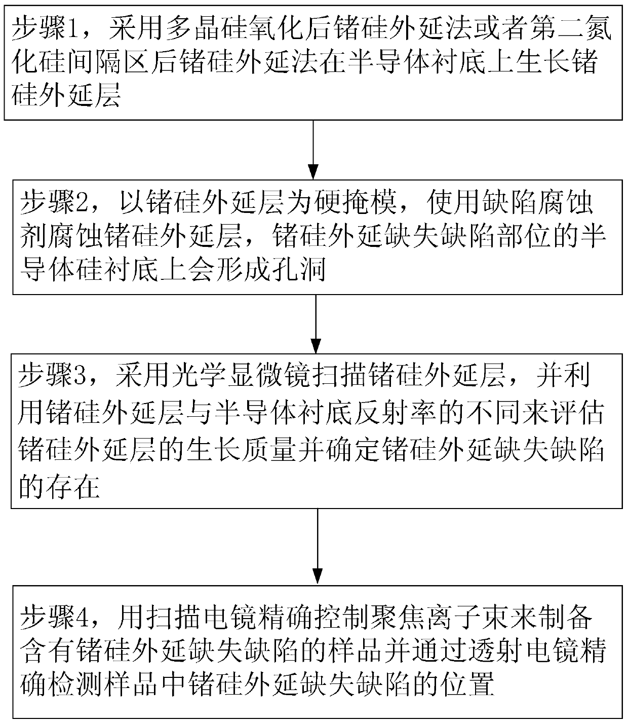
[0024] The present invention is described in detail below in conjunction with accompanying drawing:

[0025] Such as figure 1 Shown, a kind of method of detection embedded silicon germanium epitaxial missing defect of the present invention comprises the following steps:

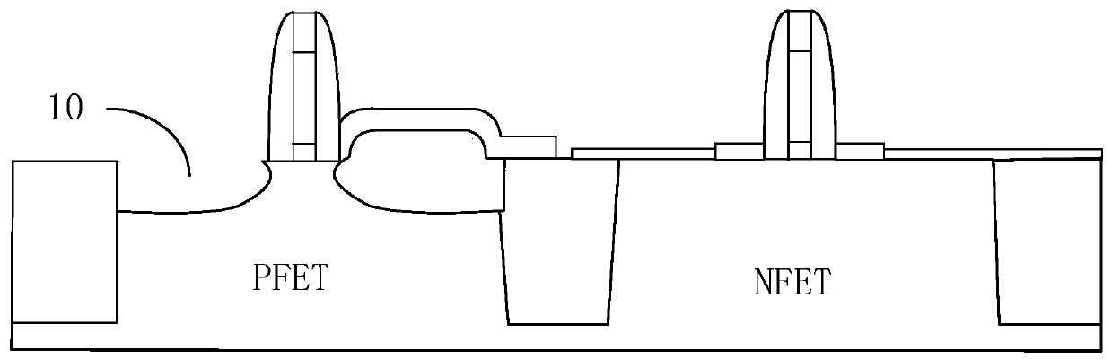
[0026] Step 1, using silicon germanium epitaxy after polysilicon oxidation or silicon germanium epitaxy after the second silicon nitride spacer to grow a silicon germanium epitaxial layer on the semiconductor silicon substrate; preferably, the silicon germanium epitaxial layer has a thickness of 100- 1000 Angstroms. At this time, due to the influence of the embedded SiGe process, some regions on the silicon germanium epitaxial layer may have deletion defects, such as figure 2 There are missing defect sites 10 on the SiGe epitaxial layer shown in .

[0027] Specifically, the silicon germanium epitaxy method after polysilicon oxidation refers to the U-shaped silicon germanium epitaxy process after polysilic...


PUM

PropertyMeasurementUnit
thicknessaaaaaaaaaa

Abstract

The invention discloses a method for detecting missing defects of an embedded germanium-silicon epitaxy. The method comprises the following steps: 1, growing a germanium-silicon epitaxial layer on a semiconductor silicon substrate by adopting a germanium-silicon epitaxial method after polysilicon oxidation or a germanium-silicon epitaxial method after a second silicon nitride spacer region; 2, corroding the germanium-silicon epitaxial layer by using a defect corrosive agent, so that holes are formed on the semiconductor silicon substrate at a missing defected part; 3, scanning the germanium-silicon epitaxial layer, evaluating the growth quality of the germanium-silicon epitaxial layer, and determining that the missing defected part exists; and 4, preparing a sample having the missing defected part, and precisely detecting the position of the missing defected part in the sample through a transmission electron microscope. According to the invention, defects generated by the technology can be found in time in the processes of developing and producing the embedded germanium-silicon epitaxy; specific and effective observation can be carried out; and thus, the problem that the device yield is decreased due to the missing defected part in a semiconductor device in the prior art can be effectively solved.

Description

technical field [0001] The invention relates to the field of semiconductor manufacturing, in particular to a method for detecting missing defects in embedded silicon germanium epitaxy. Background technique [0002] After the development of semiconductor manufacturing technology to the nanometer scale, proportional reduction technology is facing more and more severe challenges. Various new technologies must be used to improve the performance of transistors. Among them, strained silicon (Strained Silicon) technology has been widely used, embedded Silicon germanium (Embedded SiGe) is one of the solutions. [0003] Embedded SiGe source-drain technology improves the hole mobility of PMOSFET by generating uniaxial compressive stress in the channel, thereby improving its current drive capability. The principle is: by etching grooves on Si, the SiGe layer is selectively epitaxially grown. Because the SiGe lattice constant does not match Si, the Si lattice is stretched in the vertic...

Claims


Application Information

Patent Timeline
Patent Type & Authority Patents(China)
IPC IPC(8): H01L21/66
CPCH01L22/12
Inventor 张红伟周海峰
Owner SHANGHAI HUALI INTEGRATED CIRCUTE MFG CO LTD
Why Eureka
Try Eureka