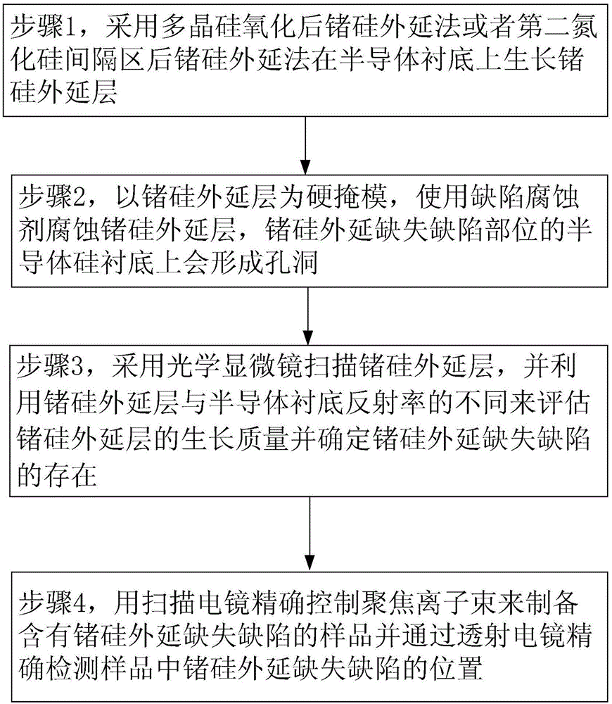
Method for detecting missing defects of embedded germanium-silicon epitaxy
An embedded silicon-germanium and silicon-germanium epitaxy technology, used in semiconductor/solid-state device testing/measurement, electrical components, circuits, etc., can solve problems such as low probability of catching defects, shortened development cycle, surface roughness, etc.
- Summary
- Abstract
- Description
- Claims
- Application Information
AI Technical Summary
Problems solved by technology
Method used
Image
Examples
Embodiment Construction
[0024] The present invention is described in detail below in conjunction with accompanying drawing:
[0025] Such as figure 1 Shown, a kind of method of detection embedded silicon germanium epitaxial missing defect of the present invention comprises the following steps:
[0026] Step 1, using silicon germanium epitaxy after polysilicon oxidation or silicon germanium epitaxy after the second silicon nitride spacer to grow a silicon germanium epitaxial layer on the semiconductor silicon substrate; preferably, the silicon germanium epitaxial layer has a thickness of 100- 1000 Angstroms. At this time, due to the influence of the embedded SiGe process, some regions on the silicon germanium epitaxial layer may have deletion defects, such as figure 2 There are missing defect sites 10 on the SiGe epitaxial layer shown in .
[0027] Specifically, the silicon germanium epitaxy method after polysilicon oxidation refers to the U-shaped silicon germanium epitaxy process after polysilic...
PUM
 Abstract
Description
Claims
Application Information


