

TFT (Thin Film Transistor) array substrate, manufacturing method and display device
An array substrate and via hole technology, applied in the field of display device manufacturing, can solve problems such as pixel electrode breakage and product yield decline
- Summary
- Abstract
- Description
- Claims
- Application Information
AI Technical Summary
Problems solved by technology
Method used
Image

Examples
Embodiment Construction
[0021] The following will clearly and completely describe the technical solutions in the embodiments of the present invention with reference to the accompanying drawings in the embodiments of the present invention. Obviously, the described embodiments are only some, not all, embodiments of the present invention. Based on the embodiments of the present invention, all other embodiments obtained by persons of ordinary skill in the art without making creative efforts belong to the protection scope of the present invention.
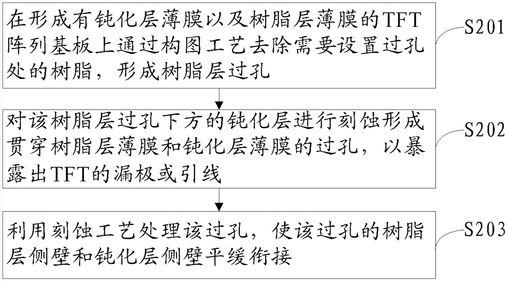
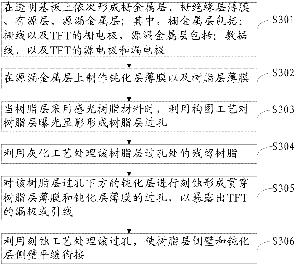
[0022] An embodiment of the present invention provides a method for manufacturing a TFT array substrate, such as figure 2 shown, including:
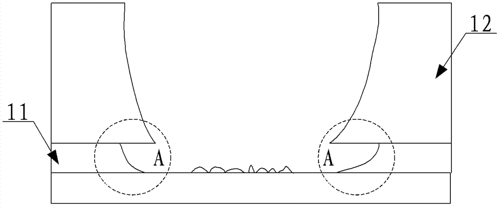
[0023] S201 , on the TFT array substrate on which the passivation layer thin film and the resin layer thin film are formed, the resin where the via hole needs to be provided is removed through a patterning process, so as to form the resin layer via hole.
[0024] S202. Etching the passivation layer below the resin laye...
PUM
 Abstract
Description
Claims
Application Information