Manufacturing process of back-drilled zero residual copper pile on PCB substrate

A manufacturing process and back-drilling technology, applied in printed circuit manufacturing, printed circuit components, reduction of crosstalk/noise/electromagnetic interference (etc.) And other issues

Inactive Publication Date: 2019-02-22
GUANGZHOU TERMBRAY ELECTRONICS TECH CO LTD
View PDF4 Cites 9 Cited by
  • Summary
  • Abstract
  • Description
  • Claims
  • Application Information

AI Technical Summary

Problems solved by technology

If the excess copper is not removed, when the frequency of the circuit signal increases to a certain height (usually above 5G), the excess copper plating is equivalent to the antenna, generating signal radiation that interferes with other surrounding signals, and in severe cases will affect the circuit For the normal operation of the system, in order to reduce this impact, the s...

Method used


Image

  • Manufacturing process of back-drilled zero residual copper pile on PCB substrate
  • Manufacturing process of back-drilled zero residual copper pile on PCB substrate
  • Manufacturing process of back-drilled zero residual copper pile on PCB substrate

Examples


Embodiment 1

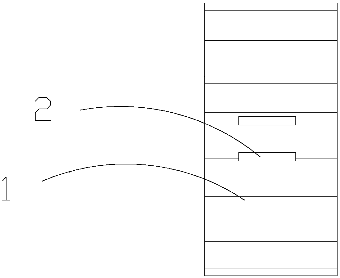
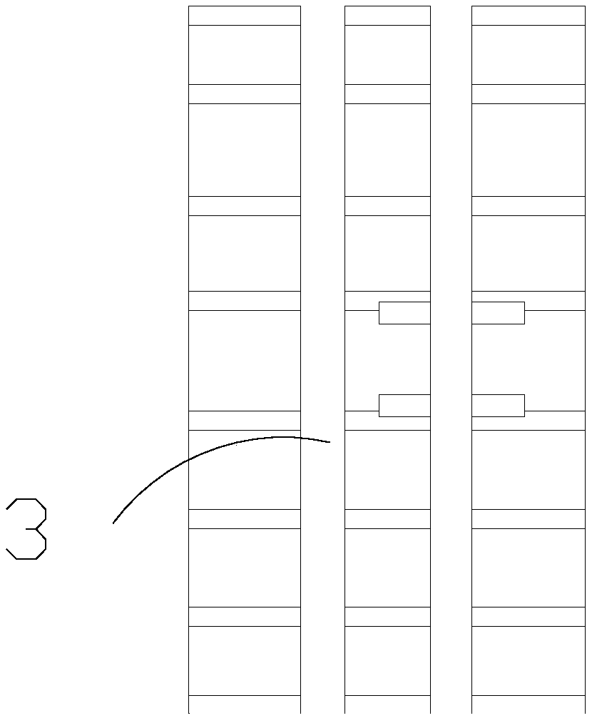
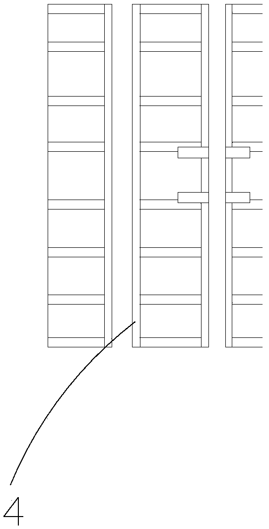
[0051] Such as Figure 1-5 As shown, the manufacturing process of the back-drilling zero residual copper pile on the PCB substrate, the specific process steps are:

[0052] a. Prepare a 4-layer circuit board, that is, have at least four conductive copper layers 1 inside it, preset two sets of disconnection layers at selected positions, and place dissolvable sheets 2 on the upper and lower sides of the disconnection layer;

[0053] b. pressing the raw material in step a into a semi-finished product;

[0054] c. Carry out mechanical drilling on the selected position to form the back drilling hole 3;

[0055] d. Coating polymer conductive film 4 in the hole after drilling;

[0056] e. Coating the dissolving solution for the dissolvable sheet in the polymer conductive film, dissolving the dissolving sheet and taking away the corresponding position of the polymer conductive film 4 to form a fault gap 5;

[0057] f. electroplating and metallizing the remaining polymer conductive ...


PUM


Abstract

The invention provides a manufacturing process of a back-drilled zero residual copper pile on a PCB substrate. The specific process includes the following steps: preparing an N-layer circuit board, wherein N>=4; longitudinally presetting A groups of disconnecting layers at a selected position, wherein A>=1; placing a soluble material on upper and lower sides of the disconnecting layers; pressing araw material in the step a into a PCB semi-finished product; mechanically drilling the PCB semi-finished product; coating the drilled holes with a polymer conductive film; dissolving the soluble material to remove to the polymer conductive film on a soluble sheet; electroplating and metallizing the remaining polymer conductive film through electroplating; and subjecting the semi-finished productin the f step to pattern plating and film stripping and etching. In the existing design scheme, through-holes that transmit a single signal are formed through mechanical back-drilling, and has a certain length of residual copper pile which interfere with signal transmission on high speed PCBs. The process can form multi-functional holes through a chemical method, a zero-residue copper pile can beachieved, which can meet the signal transmission of the high-speed PCBs. The method can be used to make back holes or multifunctional holes, and the same hole can transmit signals of two or more networks.

Description

technical field [0001] The invention relates to the field of circuit substrate optimization, in particular to a manufacturing process of back-drilling zero residual copper piles on a PCB substrate. Background technique [0002] With the development of data communication and multimedia service requirements, users are increasingly dissatisfied with a single communication method that only communicates through voice. People hope that mobile communication systems can provide a wider range of services, such as Internet access, image transmission, and video on demand. , data mutual transmission, and even watch data or multimedia services such as TV programs in real time. At the same time, it is also hoped to develop from the current communication between people to the communication between people and machines, and even between machines and machines. For this reason, the fourth generation mobile communication (4G) that meets the needs of mobile data, mobile computing and mobile mult...

Claims


Application Information

Patent Timeline
IPC IPC(8): H05K3/42H05K1/02
CPCH05K3/429H05K1/0216
Inventor 周国新朱运辉唐兵英
Owner GUANGZHOU TERMBRAY ELECTRONICS TECH CO LTD
Why Eureka
Try Eureka