Semiconductor device and forming method thereof

A semiconductor and device technology, applied in the field of semiconductor devices and their formation, can solve problems such as complex processes and achieve the effect of simplifying the process

Inactive Publication Date: 2019-03-05
SEMICONDUCTOR MANUFACTURING INTERNATIONAL (BEIJING) CORP +1
View PDF8 Cites 3 Cited by
  • Summary
  • Abstract
  • Description
  • Claims
  • Application Information

AI Technical Summary

Problems solved by technology

[0004] However, the process of the existing

Method used


Image

  • Semiconductor device and forming method thereof
  • Semiconductor device and forming method thereof
  • Semiconductor device and forming method thereof

Examples


Embodiment Construction

[0031] As mentioned in the background art, the process of forming semiconductor devices in the prior art is relatively complicated.

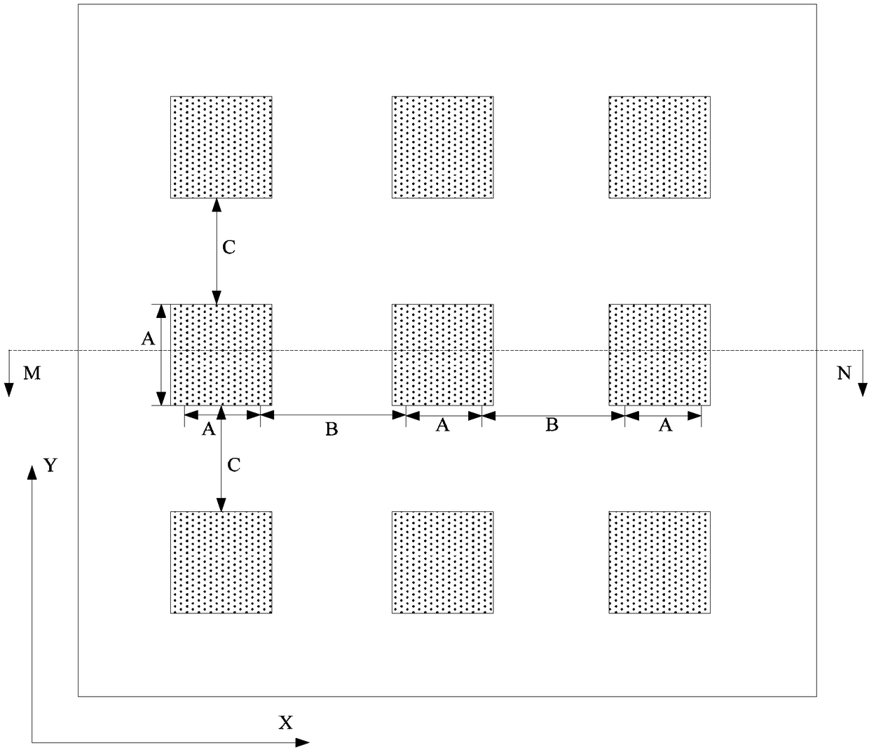
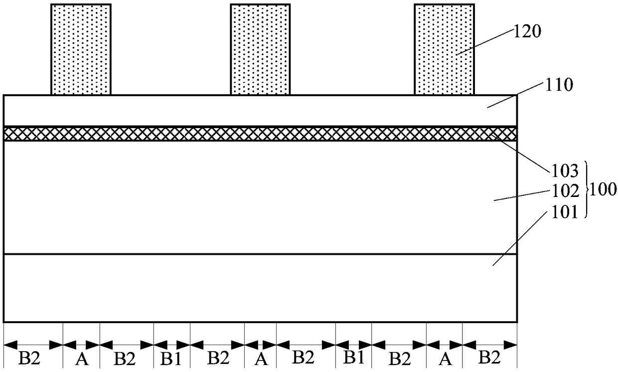
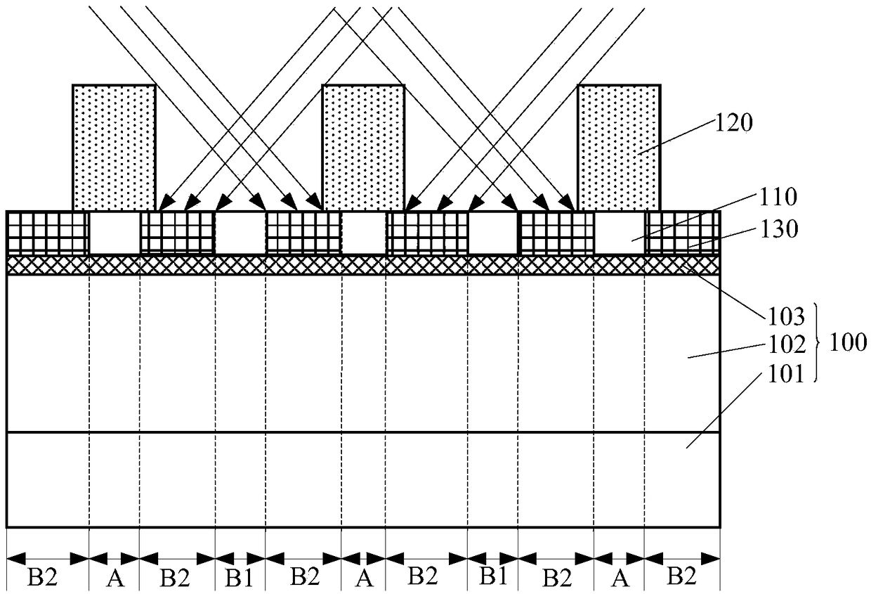
[0032] A method for forming a semiconductor device, comprising: providing a material layer to be etched; forming a plurality of discrete sacrificial layers on the material layer to be etched; forming a first side wall and a second side wall on the side wall of the sacrificial layer, the first Both ends of the second side wall are respectively connected with the adjacent first side wall, the second side wall and the first side wall are in a ring structure; the second side wall is removed; after the second side wall is removed, the sacrificial layer is removed; the sacrificial layer is removed After layering, the material layer to be etched is etched using the first sidewall as a mask to form a pattern in the material layer to be etched.

[0033] However, the process of the semiconductor device formed by the above-mentioned method is relatively co...


PUM

PropertyMeasurementUnit
Thicknessaaaaaaaaaa
Thicknessaaaaaaaaaa

Abstract

The invention relates to a semiconductor device and a forming method thereof. The method comprises the following steps: forming a fragmented top mask structure in a first region of a bottom mask material layer, wherein the top mask structure comprises a top mask layer and the top mask structure also stretches to partial surface of an edge region; using the top template structure as the mask to perform modifying processing on the edge region and a third region of the bottom mask material layer; forming a modifying layer in the edge region and the third region of the bottom template material layer; removing the modifying layer and forming a groove in the edge region and the third region of the bottom template material layer so that the first region and the middle region of the bottom mask material form a bottom mask layer between adjacent grooves. The method simplifies the imaging craft process.

Description

technical field [0001] The invention relates to the field of semiconductor manufacturing, in particular to a semiconductor device and a forming method thereof. Background technique [0002] In the process of manufacturing semiconductor devices, the patterning process is an important process step. [0003] The patterning process generally includes: providing a material layer to be etched; forming a mask layer on the material layer to be etched; using the mask layer as a mask to etch the material layer to be etched, forming target graphics. During the patterning process, the pattern quality of the mask layer has a great influence on the quality of the target pattern. [0004] However, the process of the existing patterning process is relatively complicated. Contents of the invention [0005] The problem solved by the present invention is to provide a semiconductor device and its forming method to simplify the process of patterning. [0006] In order to solve the above pr...

Claims


Application Information

Patent Timeline
IPC IPC(8): H01L21/033
CPCH01L21/0337
Inventor 张海洋常荣耀
Owner SEMICONDUCTOR MANUFACTURING INTERNATIONAL (BEIJING) CORP
Why Eureka
Try Eureka