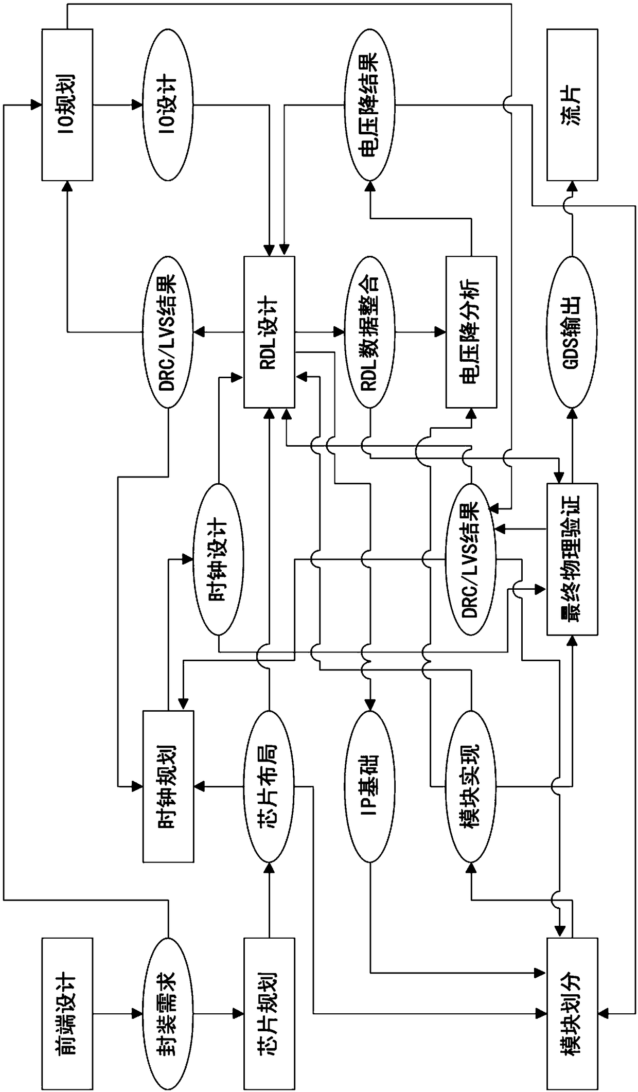
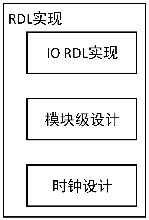
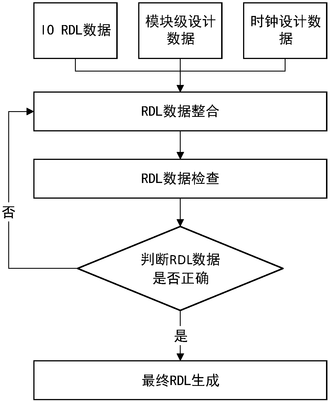
[0026] The present invention discloses an efficient RDL design method for semi-customized design of the back end of an integrated circuit. The specific implementation of the present invention will be further described below in conjunction with preferred embodiments.
[0027] It is worth mentioning that those skilled in the art should note that the "RDL" (Redistribution Layer) involved in the patent application of the present invention is defined as "rewiring layer"; the "GDS" involved in the patent application of the present invention is defined as a A "data format during chip production"; "LVS" involved in the patent application of this invention is defined as "comparison of layout and schematic diagram"; "DRC" involved in the patent application of this invention is defined as "design rule check"; The "IP" involved in the patent application of the present invention is defined as "intellectual property"; the "IO" involved in the patent application of the present invention is defined as "input and output pins".
[0028] See attached Figure 1 to Figure 5 , figure 1 Shows the system structure of the high-efficiency RDL design method for the semi-customized design of the integrated circuit back-end, Figure 2 to Figure 4 Respectively show the relevant schematic diagrams of each step of the high-efficiency RDL design method for the semi-custom design of the integrated circuit back-end, Figure 5 The visual result of the final RDL tape-out filling of the high-efficiency RDL design method of the semi-customized design of the integrated circuit back-end is shown.
[0029] Preferably, the high-efficiency RDL design method for semi-customized design of the integrated circuit back-end includes the following steps:
[0030] Step S1: Carry out overall chip planning based on RDL design requirements;
[0031] Step S2: Generate final RDL design data based on the chip global planning result in step S1.
[0032] Among them, step S1 specifically includes the following steps:
[0033] Step S1.1: Perform IO RDL design and form IO RDL data to complete the design of the chip's input and output pins;
[0034] Step S1.2: Perform module-level design and form module-level design data to complete the design of the chip other than RDL;
[0035] Step S1.3: Perform clock design and form clock design data to complete the clock design of the chip.
[0036] Among them, step S2 specifically includes the following steps:
[0037] Step S2.1: Integrate the aforementioned IO RDL data, module-level design data, and clock design data to form complete RDL design data;
[0038] Step S2.2: Check the above-mentioned RDL complete design data to determine whether the data is accurate, if the judgment is true (the data can pass the check), go to step S2.3, otherwise go to step S1.1;
[0039] Step S2.3: Generate final data for RDL design according to the above-mentioned complete RDL design data.
[0040] Among them, step S2.3 specifically includes the following steps:
[0041] Step S2.3.1: Design the final RDL metal line according to the above-mentioned complete RDL design data;
[0042] Step S2.3.2: Connect the final RDL metal wire;
[0043] Step S2.3.3: Perform tape-out filling according to the final RDL metal wire that is connected.
[0044] According to the above-mentioned preferred embodiment, the high-efficiency RDL design method for the semi-customized design of the back end of the integrated circuit disclosed in the patent application of the present invention is specifically described as follows.
[0045] 1. The overall design and planning steps.
[0046] Based on advanced RDL design requirements, a global chip plan based on RDL design is required. The plan is mainly divided into four parts, namely RDL implementation, IO RDL implementation (design) part, module-level design part and clock design part, such as figure 2 Shown.
[0047] Among them, IO RDL is designed to complete the design of chip input and output pins. After the introduction of IO RDL design, all input and output pins of the chip are completed by IO RDL.
[0048] Among them, module-level design is used to complete all designs other than RDL. Since RDL is a part of the complete chip design, designs other than RDL account for most of the chip design, so designs other than RDL design need to be implemented separately.
[0049] Among them, the clock design is used for the clock design related to RDL. With the introduction of RDL technology, the clock design part of the chip has to be completed using RDL, otherwise a lot of manufacturing resources will be wasted and the design cost will be unacceptable.
[0050] Among them, RDL implementation is used to complete the integration of all RDL data and non-RDL data to obtain the complete design data of the final chip design.
[0051] 2. The final RDL generation step.
[0052] Based on the data obtained in the overall design planning step, the final RDL design data is generated, such as image 3 Shown.
[0053] The final RDL generation is divided into three stages. First, the RDL raw data needs to be integrated. Since the data obtained in the overall design planning steps are relatively independent design data in each design link, the data needs to be integrated.
[0054] Then, it is necessary to check the correctness of the integrated data. It is necessary to ensure that the initial data has no problems after the integration, otherwise, it is necessary to return to the overall design and planning steps for error correction.
[0055] Finally, generate the final data of the RDL design.
[0056] 3. The final data generation steps of RDL design.
[0057] The final data of RDL design requires the following 3 steps, such as Figure 4 Shown.
[0058] Since each design part is connected to each other, in step 1 and step 2, only the design of the design part itself and the splicing between independent data are carried out, and the design of each design link is realized through the realization of the final RDL metal line Winding is performed, and all windings are implemented through RDL.
[0059] After the design of all RDL metal lines is completed, the connections between different layers of metal need to be made through through holes, and finally all the metal lines are connected.
[0060] After all the RDL wires are wound and connected, the chip production process requires production-related processing. This processing is to fill the blank area of the chip with metal to achieve the purpose of successful manufacturing. Therefore, the final step is the flow of the final RDL. The final result of RDL design is as Figure 5 Shown.
[0061] It is worth mentioning that, according to the above-mentioned preferred embodiment, the semi-customized design method for the back-end of the integrated circuit disclosed in the patent application of the present invention has a technical point that is based on the advanced nature, completeness and maturity of the design method. The end design team can effectively avoid invalid work and reduce the number of design iterations, and ultimately shorten the entire chip design cycle. This method is suitable for various back-end design projects with different design requirements, and has good versatility and advancement.
[0062] For those skilled in the art, it is still possible to modify the technical solutions described in the foregoing embodiments, or to equivalently replace some of the technical features, any modifications made within the spirit and principle of the present invention, Equivalent replacements, improvements, etc., should all be included in the protection scope of the present invention.