A method for improving the abnormality of the lift OFF process pattern of the thick metal layer

A metal layer, thick metal technology, applied in the manufacture of electrical components, circuits, semiconductor/solid-state devices, etc., can solve problems such as reducing the thickness of photoresist, and achieve the effect of improving cracks, reducing difficulty, and reducing thickness

A metal layer, thick metal technology, applied in the manufacture of electrical components, circuits, semiconductor/solid-state devices, etc., can solve problems such as reducing the thickness of photoresist, and achieve the effect of improving cracks, reducing difficulty, and reducing thickness

CN109461652BActive Publication Date: 2021-11-02WUXI ZHONGWEI JINGYUAN ELECTRONIC CO LTD

Image

  • A method for improving the abnormality of the lift OFF process pattern of the thick metal layer
  • A method for improving the abnormality of the lift OFF process pattern of the thick metal layer
  • A method for improving the abnormality of the lift OFF process pattern of the thick metal layer

Examples


Embodiment Construction

[0038] The present invention will be further described below in conjunction with specific drawings and embodiments.

[0039] The present invention is not limited to the following embodiments, and each figure referred to in the following description is provided for understanding the content of the present invention, that is, the present invention is not limited to the structures illustrated in each figure.

[0040] A method for improving abnormal pattern of thick metal layer LIFT OFF process, comprising the steps of:

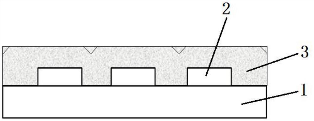
[0041] like figure 1 As shown, step 1. Photoresist coating: select a wafer substrate 1 patterned by a front-side process, coat photoresist 3 on the surface of the wafer substrate 1, and the thickness of the photoresist 3 is 6±0.5um;

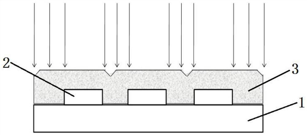
[0042] like figure 2 As shown, step 2. Photoresist exposure: under the shielding of the patterned photoresist plate, the photoresist 3 is exposed;

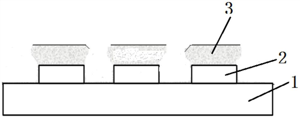
[0043] like image 3 As shown, step 3. Photoresist development: develop the p...


PUM


Abstract

The invention belongs to the technical field of semiconductor integrated circuits, and relates to a method for improving abnormal pattern of thick metal layer LIFT OFF process, specifically photoresist coating-photoresist exposure-photoresist development-thick metal layer deposition-blue paste Film-blue film stripping-photoresist stripping; the LIFT OFF process method of the present invention, in the metal deposition process, adopts low-temperature process to avoid photoresist collapse, adopts low-speed multiple evaporation process, combined with blue film-assisted stripping method , not only reduces the thickness of the photoresist, but also avoids the oblique collapse of the thicker metal layer (above 3um) on the photoresist and the pattern abnormality caused by the crack of the photoresist, so as to finally realize the thick metal layer LIFT OFF process.

Description

technical field [0001] The invention relates to a method for a LIFT OFF process, in particular to a method for improving the pattern abnormality of a thick metal layer LIFT OFF process, and belongs to the technical field of semiconductor integrated circuit technology. Background technique [0002] In the integrated circuit process, the metal titanium-nickel-silver (Ti-Ni-Ag) needs to be selectively covered (that is, it needs to be patterned), and the dry etching cannot remove the metal nickel-silver by etching, and the patterned metal titanium-nickel silver cannot be obtained. Silver, wet etching Because there is metal aluminum on the surface of the wafer, the aluminum will be corroded at the same time, and the uniformity of the corrosion is poor, so it is difficult to realize the mass production process. In order to solve this problem, the current processing technology adopts the metal LIFT OFF process, that is, the metal photoresist stripping technology. [0003] The conv...

Claims


Application Information

Patent Timeline
02 Nov 2021
Publication
CN109461652B
IPC
H01L21/3205
CPC
H01L21/32051
Inventors
孙建洁; 张世权