Chip pin correction tooling and chip installation method

A chip mounting and chip technology, which is applied to the assembly of printed circuits with electrical components, electrical components, and printed circuit manufacturing. It can solve the problem of poor bonding between the solder on the surface of the PCB and the pins of the western chip, affecting soldering reliability, and inaccurate positioning. question

Inactive Publication Date: 2019-03-12
CHANGCHUN INST OF OPTICS FINE MECHANICS & PHYSICS CHINESE ACAD OF SCI
View PDF6 Cites 6 Cited by
  • Summary
  • Abstract
  • Description
  • Claims
  • Application Information

AI Technical Summary

Problems solved by technology

[0003] However, when installing a chip with lead pins, usually the pins of the chip and the pads on the surface of the PCB cannot be accurately positioned, resulting in poor bondi

Method used


Image

  • Chip pin correction tooling and chip installation method
  • Chip pin correction tooling and chip installation method
  • Chip pin correction tooling and chip installation method

Examples


Embodiment Construction

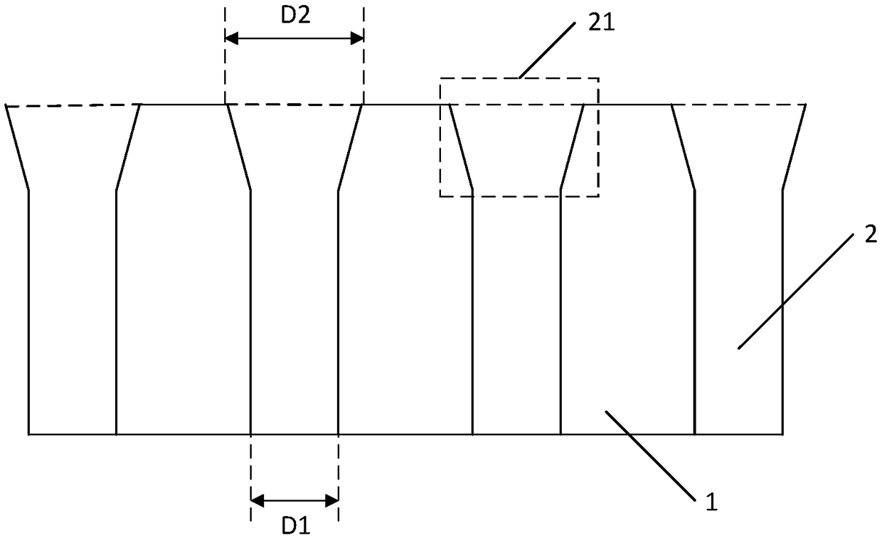
[0035] The core of the invention is to provide a chip lead correction tool. For chips with lead pins, the rigidity of the lead pins is poor, and the lead pins are prone to complete deformation and deflection during transportation and storage, so that there is no contact between the pins of the chip and the pads on the surface of the PCB. Precise positioning, resulting in poor bonding between the solder and the pins, which in turn leads to problems such as low solder joint strength, which affects the reliability of soldering.

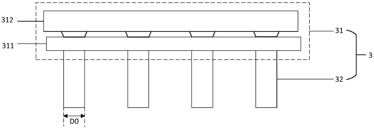
[0036] And a kind of chip lead correction tool provided by the present invention comprises a substrate and a guide hole positioned on the surface of the substrate; wherein the guide hole corresponds to the pin of the chip to be installed, and the lead of the chip to be installed is a lead post, and the lead post is in the The surface of the chip to be mounted forms a lead post array, and the guide holes form a guide hole array in the substrate, and the g...


PUM


Abstract

The invention discloses a chip pin correction tooling. Since a guiding hole array composed of the guiding holes corresponds to a lead column array composed of lead columns, the guiding holes are onlyslightly larger than the diameter of the lead columns, and the texture of the lead columns is soft, the lead columns can be slowly pressed into the guiding holes of the calibration tooling to adjust the spacing among the lead columns and the morphology of the lead columns, so as to make the spacing among the lead columns and the topography of the lead columns meet preset standards; therefore, accurate positioning between chip pins and a PCB surface bonding pad can be realized, the combination degree of a solder and the pins is improved, the solder joint strength is improved, and the solderingreliability is improved. The invention also provides a chip installation method. The spacing among the lead columns and the topography of the lead columns can be corrected through the correction tooling; therefore, the accurate positioning between the chip pins and the PCB surface bonding pad can be realized when soldering the chip to the surface of the PCB, the combination degree of the solder and the pins is improved, the solder joint strength is improved, and the soldering reliability is improved.

Description

technical field [0001] The invention relates to the technical field of electronic assembly, in particular to a chip pin calibration tool and a chip mounting method. Background technique [0002] In the assembly process of printed boards, especially in the assembly process of printed boards of aerospace products, due to the need for high reliability, chips with lead pins are usually used, such as CI-CGA (Ceramics Integration-Cone Grid Array ) packaged chip as the chip in the circuit board. Chips in CI-CGA package form have a series of advantages such as good thermal matching performance, strong resistance to mechanical vibration and high pin integration, and are widely used in high-reliability occasions. [0003] However, when installing a chip with lead pins, usually the pins of the chip and the pads on the surface of the PCB cannot be accurately positioned, resulting in poor bonding between the solder on the surface of the PCB and the pins of the western chip, resulting in...

Claims


Application Information

Patent Timeline
IPC IPC(8): H05K13/00H05K13/04H05K3/34
CPCH05K3/3447H05K13/0092H05K13/04
Inventor 张伟王威石宝松
Owner CHANGCHUN INST OF OPTICS FINE MECHANICS & PHYSICS CHINESE ACAD OF SCI
Why Eureka
Try Eureka