Semiconductor device
A semiconductor, conductive type technology, applied in the direction of semiconductor devices, electrical components, circuits, etc., can solve the problems of voltage resistance fluctuation, poor reliability, charge imbalance and so on
- Summary
- Abstract
- Description
- Claims
- Application Information
AI Technical Summary
Problems solved by technology
Method used
Image
Examples
no. 1 approach
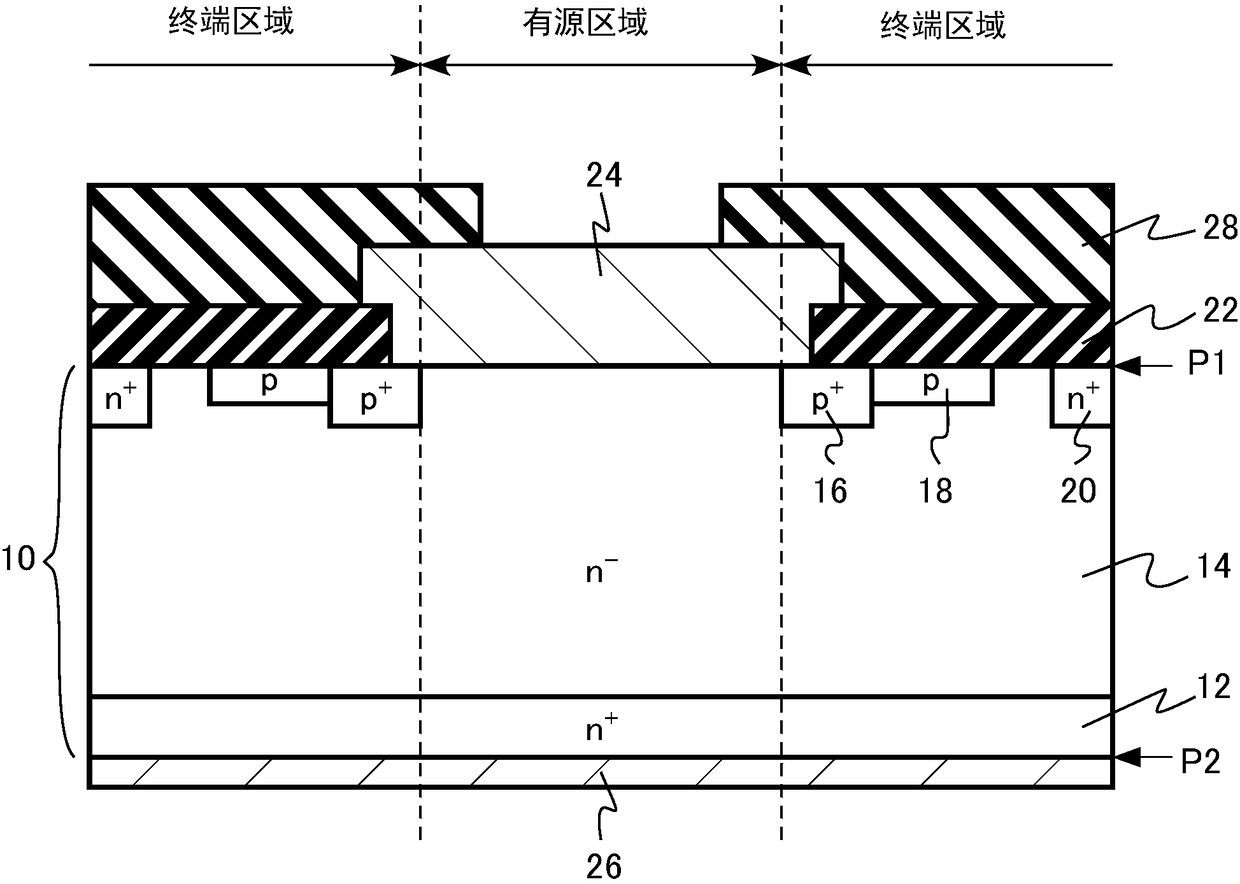
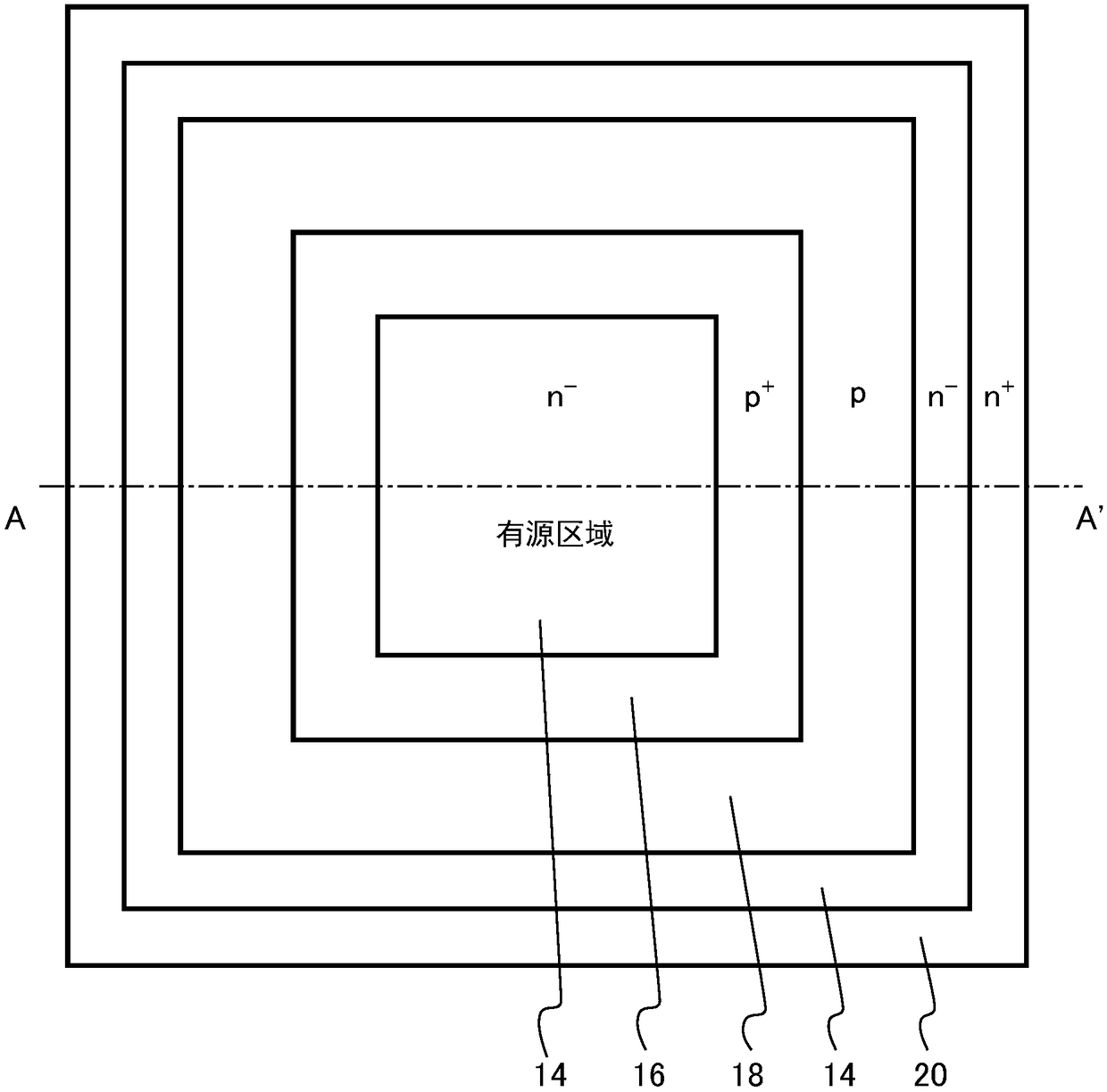
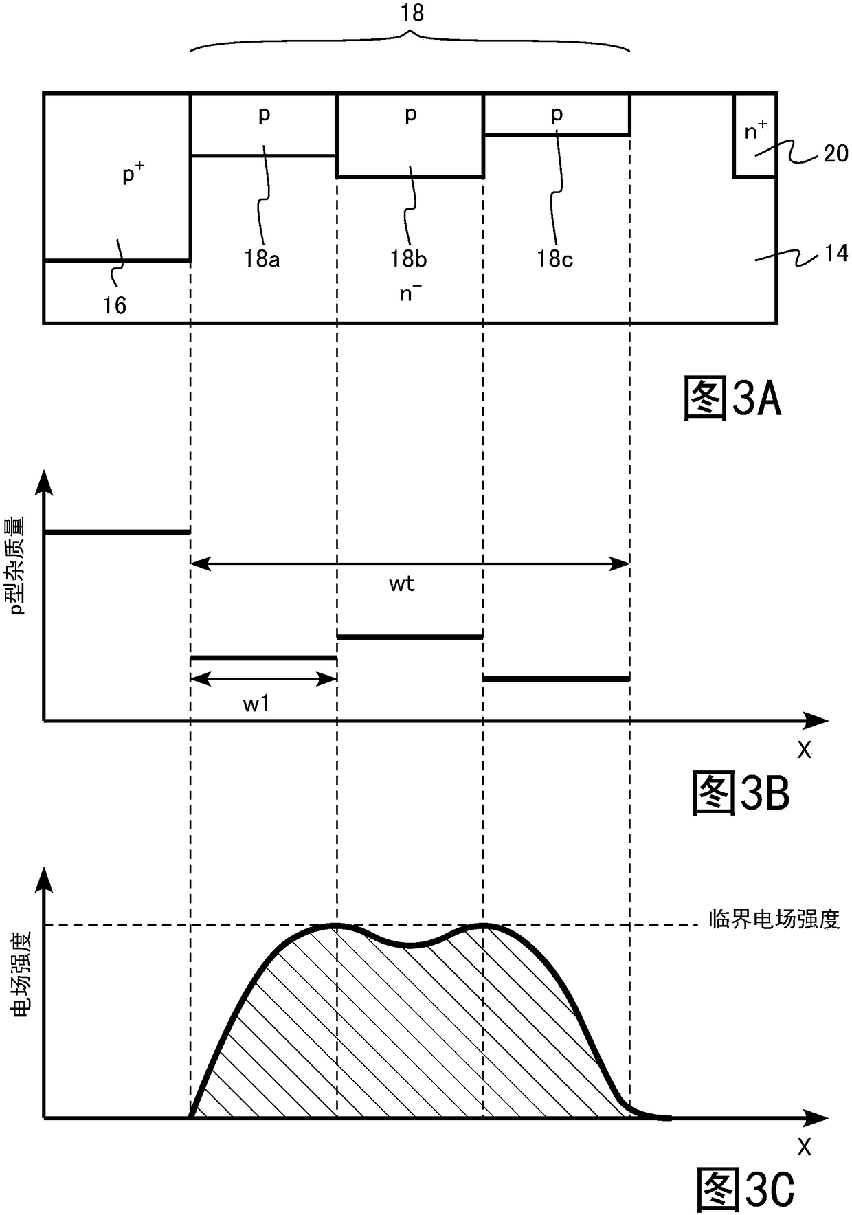
[0022] The semiconductor device according to the first embodiment includes: a semiconductor layer having a first surface and a second surface; a first electrode provided in contact with the first surface; a second electrode provided in contact with the second surface; a semiconductor region disposed in the semiconductor layer; a ring-shaped second semiconductor region of the second conductivity type disposed between the first semiconductor region and the first surface, connected to the first surface, and electrically connected to the first electrode; and The third semiconductor region of the second conductivity type is arranged around the second semiconductor region, is arranged between the first semiconductor region and the first surface, is in contact with the first surface, has the first region, and is farther away from the second semiconductor region than the first region. A second region of the semiconductor region, a third region further away from the second semiconductor...
no. 2 approach
[0081] The semiconductor device of the second embodiment differs from the first embodiment in that at least a part of the first region has a second conductivity type impurity concentration lower than that of at least a part of the second region. Hereinafter, descriptions will be omitted for parts that overlap with those of the first embodiment.
[0082] Figure 6A , Figure 6B , Figure 6C It is an enlarged schematic cross-sectional view of the terminal region of the semiconductor device according to the second embodiment. Figure 6A for the sectional view, Figure 6B is a graph showing the p-type impurity amount of each impurity region, Figure 6C is a graph showing the electric field intensity distribution.
[0083] In the SBD of the second embodiment, the depths of the first region 18a, the second region 18b, and the third region 18c are substantially constant.
[0084] The p-type impurity concentration at any position of the first region 18a is lower than the p-type ...
no. 3 approach
[0089] The semiconductor device according to the third embodiment differs from the first embodiment in that a fourth semiconductor region of the first conductivity type having a higher impurity concentration of the first conductivity type than the first semiconductor region is provided between the first region and the first semiconductor region. different ways. Hereinafter, descriptions will be omitted for parts that overlap with those of the first embodiment.
[0090] Figure 7A , Figure 7B , Figure 7C It is an enlarged schematic cross-sectional view of the terminal region of the semiconductor device of the third embodiment. Figure 7A for the sectional view, Figure 7B is a graph showing the p-type impurity amount of each impurity region, Figure 7C is a graph showing the electric field intensity distribution.
[0091] The SBD of the third embodiment includes an n-type region 40 (fourth semiconductor region).
[0092] In the SBD of the third embodiment, the p-type i...
PUM
 Abstract
Description
Claims
Application Information
 - R&D Engineer
- R&D Manager
- IP Professional
- Industry Leading Data Capabilities
- Powerful AI technology
- Patent DNA Extraction
Browse by: Latest US Patents, China's latest patents, Technical Efficacy Thesaurus, Application Domain, Technology Topic, Popular Technical Reports.
© 2024 PatSnap. All rights reserved.Legal|Privacy policy|Modern Slavery Act Transparency Statement|Sitemap|About US| Contact US: help@patsnap.com


