Flat panel detector and its pixel driving circuit

A pixel drive circuit and flat panel detector technology, applied in circuits, instruments, televisions, etc., can solve the problems of increasing the signal-to-noise ratio of the readout signal of the flat-panel detector and easy saturation of the electricity, so as to improve the imaging quality and reduce the signal-to-noise ratio Effect

Active Publication Date: 2022-01-28
BOE TECH GRP CO LTD +1
View PDF12 Cites 0 Cited by
  • Summary
  • Abstract
  • Description
  • Claims
  • Application Information

AI Technical Summary

Problems solved by technology

However, in the flat panel detector, the charge generated by the active pixel detector induced by light is amplified by the amplifier. Under a certain power supply voltage, the capacitor is easily saturated, which may increase the signal-to-noise ratio of the readout signal of the flat panel detector, and will Will cause greater image quality problems

Method used


Image

  • Flat panel detector and its pixel driving circuit
  • Flat panel detector and its pixel driving circuit
  • Flat panel detector and its pixel driving circuit

Examples


Embodiment Construction

[0022] Embodiments of the present invention are described in detail below, examples of which are shown in the drawings, wherein the same or similar reference numerals designate the same or similar elements or elements having the same or similar functions throughout. The embodiments described below by referring to the figures are exemplary and are intended to explain the present invention and should not be construed as limiting the present invention.

[0023] The following describes the pixel driving circuit and the flat panel detector of the flat panel detector proposed by the embodiments of the present invention with reference to the accompanying drawings.

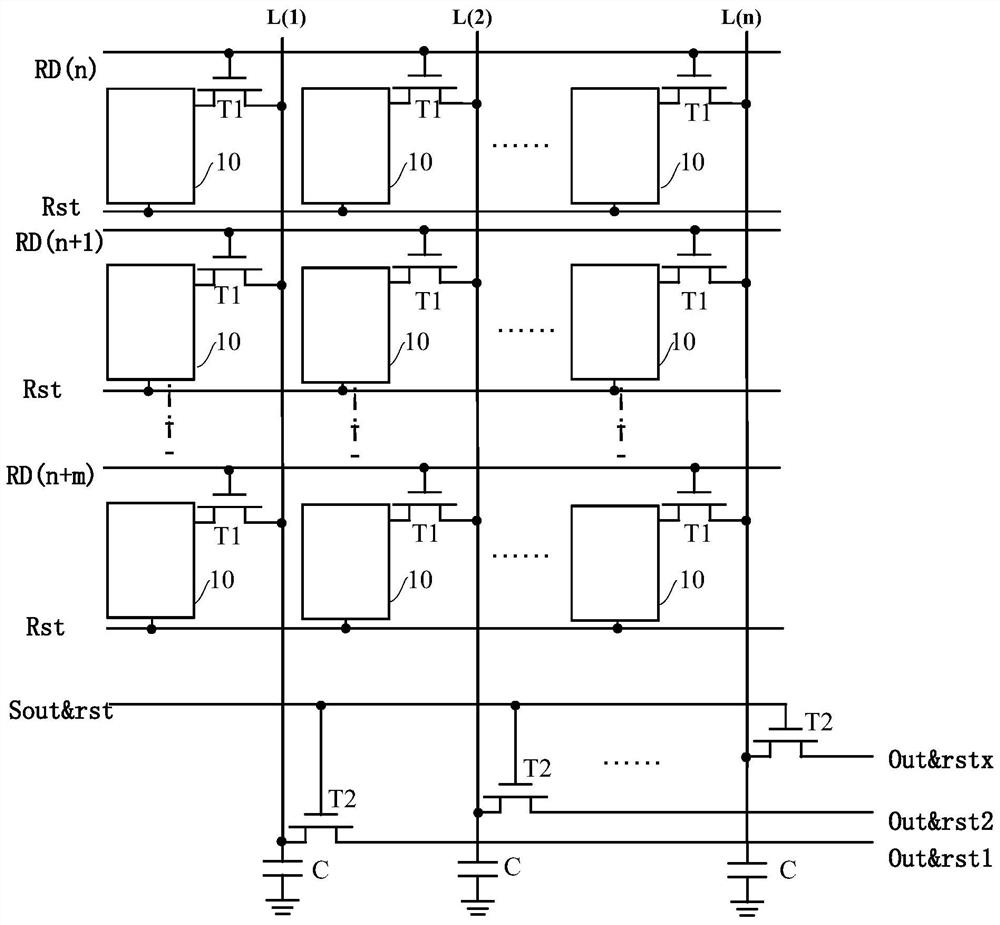
[0024] figure 1 is a schematic block diagram of a pixel driving circuit of a flat panel detector according to an embodiment of the present invention. Such as figure 1 As shown, the pixel driving circuit includes: a plurality of pixel units 10 and a plurality of capacitors C.

[0025] Wherein, a plurality of pixel units...


PUM


Abstract

The invention discloses a flat panel detector and a pixel driving circuit thereof, wherein the pixel driving circuit comprises: a plurality of pixel units arranged in an array; a plurality of capacitors connected to the plurality of pixel units in the column for storing Output the charge data generated by multiple pixel units in the column. The pixel drive circuit adopts the method of setting the storage capacitor outside the pixel area as a column storage capacitor. The size of the capacitor is no longer limited by the size of the pixel, so that it can better cooperate with the large amount of charge read out by the flat panel detector and reduce the readout of the flat panel detector. The signal-to-noise ratio of the signal can improve the image quality.

Description

technical field [0001] The invention relates to the technical field of digital imaging, in particular to a pixel driving circuit of a flat panel detector and a flat panel detector. Background technique [0002] A flat panel detector is an X-ray image detector with a photodiode array as its core. Under X-ray irradiation, the scintillator or phosphor layer of the detector converts X-ray photons into visible light, and then the array with photodiode function becomes image electrical signal, which is read out by peripheral circuit and A / D conversion, so as to obtain digitization image. It has gone through the imaging process of X-ray-visible light-charge image-digital image. [0003] However, unlike the CMOS image sensor technology based on the silicon process, the TFT process pixel circuit is limited by the process level and its own large size, and the consistency of the key TFTs in each pixel is serious. Therefore, the current flat panel detector Among them, the TFT is only...

Claims


Application Information

Patent Timeline
Patent Type & Authority Patents(China)
IPC IPC(8): H04N5/32H04N5/14H01L27/146
CPCH01L27/14663H04N5/14H04N5/32H01L27/14609G01T1/247H04N25/75H01L27/14659
Inventor 段立业李延钊
Owner BOE TECH GRP CO LTD
Why Eureka
Try Eureka