A method for fully laminating a display module

A technology for displaying modules and manufacturing methods, which is applied in the direction of material gluing, devices for coating liquid on the surface, identification devices, etc., and can solve problems such as easy displacement of components

Active Publication Date: 2021-04-30
TRULY SEMICON
View PDF5 Cites 2 Cited by
  • Summary
  • Abstract
  • Description
  • Claims
  • Application Information

AI Technical Summary

Problems solved by technology

[0005] In order to solve the above problems, the present invention provides a full lamination manufacturing method of display modules, which can solve the problem that the components to be bonded in the full lamination process are prone to displacement

Method used


Image

  • A method for fully laminating a display module
  • A method for fully laminating a display module
  • A method for fully laminating a display module

Examples


Embodiment 1

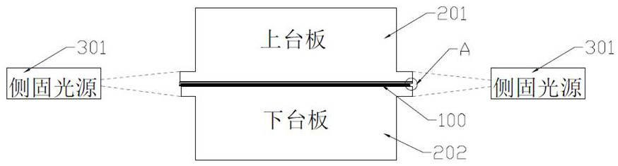
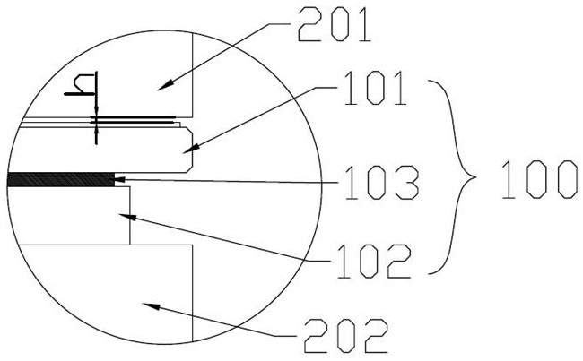
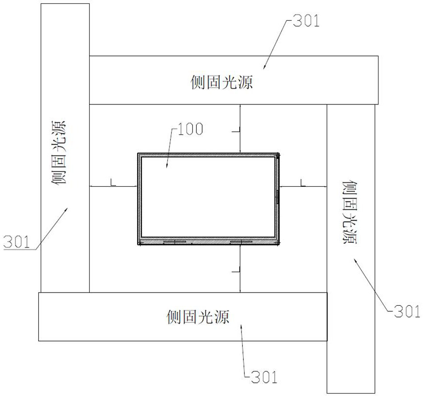
[0030] Figure 1~Figure 3 It is the accompanying drawing of the embodiment of the present invention. The invention provides a method for fully laminating a display module. The display module 100 includes a first substrate 101 and a second substrate 102 .

[0031] In this embodiment, the first substrate 101 is a touch screen, and the second substrate 102 is a display screen.

[0032] The full lamination manufacturing method of the display module 100 includes the following steps:

[0033] (1). Coating: using screen printing coating technology, using an automatic glue coating device to coat the first substrate 101 with optical glue to form an optical glue layer 103;

[0034] (2). Alignment and bonding: first use the alignment adjustment system to align the first substrate 101 and the second substrate 102 on the horizontal plane; then attach the first substrate 101 and the second substrate 102, and pass Move the alignment adjustment system to control the thickness of the dis...

Embodiment 2

[0049] Different from Embodiment 1, in this embodiment, the first substrate is a screen cover, and the second substrate is a display screen.

Embodiment 3

[0051] Different from Embodiment 1, in this embodiment, the first substrate is a display screen, and the second substrate is a screen cover or a touch screen.

[0052] Compared with the prior art, the beneficial effects of the present invention are as follows:

[0053] After the first substrate and the second substrate are aligned and bonded, the display module is directly exposed and cured at the bonding station, and the display module does not need to be moved, which simplifies the process steps. Moreover, the problem that the glue easily flows during the process of moving the display module to the next station is avoided. In addition, by exposing and curing the four sides of the display module at the same time, the four sides of the optical adhesive layer will be cured first to form a glue wall. The relative position remains unchanged.


PUM


Abstract

The invention discloses a full lamination manufacturing method of a display module. The display module includes a first substrate and a second substrate; the full lamination manufacturing method includes the following steps: (1). Coating: coating the first substrate with optical glue; (2). Alignment and bonding: first use the alignment adjustment system to align the first substrate and the second substrate on the horizontal plane; then attach the first substrate and the second substrate, and adjust the alignment by moving in the vertical direction System, control the thickness of the display module within the specified range; (3). Side curing: Use the curing device to simultaneously expose and cure the four sides of the display module located in the bonding station. In the present invention, after the first substrate and the second substrate are aligned and bonded, the display module is directly exposed and cured at the bonding station, and the display module does not need to move its position, which simplifies the process steps. Moreover, the process of moving the display module to the next station is avoided.

Description

technical field [0001] The present invention mainly relates to the technical field of display module processing technology, and more specifically relates to a method for fully laminating a display module. Background technique [0002] With the development of the economy, due to the high reliability and high transmittance of full lamination, the full lamination technology has gradually penetrated into industrial, home appliances, automotive, and three aviation (aviation, navigation, aerospace) products. Customer demands are increasing year by year, and the use of OCR and other optical adhesives for full lamination has become an irreversible technical trend. [0003] However, using OCR optical glue to fully bond the display screen and touch screen (including capacitive screens and resistive screens), the bonded components are prone to displacement after bonding. It cannot meet the customer's alignment accuracy requirements for the product. Now it is necessary to study the fu...

Claims


Application Information

Patent Timeline
Patent Type & Authority Patents(China)
IPC IPC(8): F16B11/00G09F9/00B05D3/06
CPCB05D3/06F16B11/006G09F9/00
Inventor 欧坚俊赵学辉吴振文
Owner TRULY SEMICON
Why Eureka
Try Eureka