Display module, manufacturing method thereof, and display device

A technology of display module and manufacturing method, applied in identification device, circuit device, crosstalk/noise/electromagnetic interference reduction (and other directions, can solve problems such as unfavorable bending, circuit damage, COF thickness, etc.

Inactive Publication Date: 2019-04-02
BOE TECH GRP CO LTD +1
View PDF7 Cites 14 Cited by
  • Summary
  • Abstract
  • Description
  • Claims
  • Application Information

AI Technical Summary

Problems solved by technology

[0004] Because the insulating electromagnetic material is attached to the COF, the COF is thicke

Method used


Image

  • Display module, manufacturing method thereof, and display device
  • Display module, manufacturing method thereof, and display device
  • Display module, manufacturing method thereof, and display device

Examples


Embodiment Construction

[0033] In order to make the purpose, technical solutions and advantages of the present invention clearer, the following will clearly and completely describe the technical solutions in the embodiments of the present invention with reference to the drawings in the embodiments of the present invention.

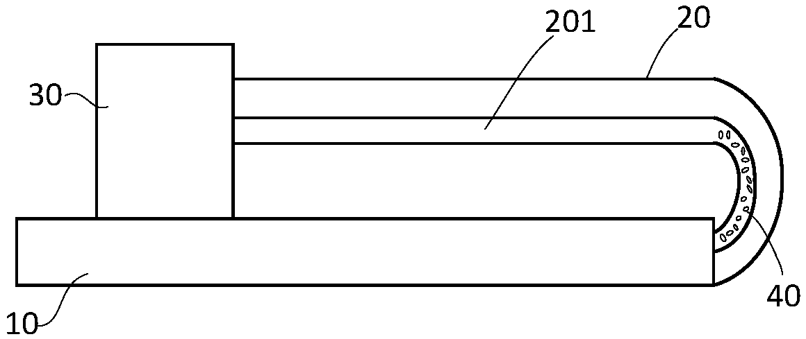
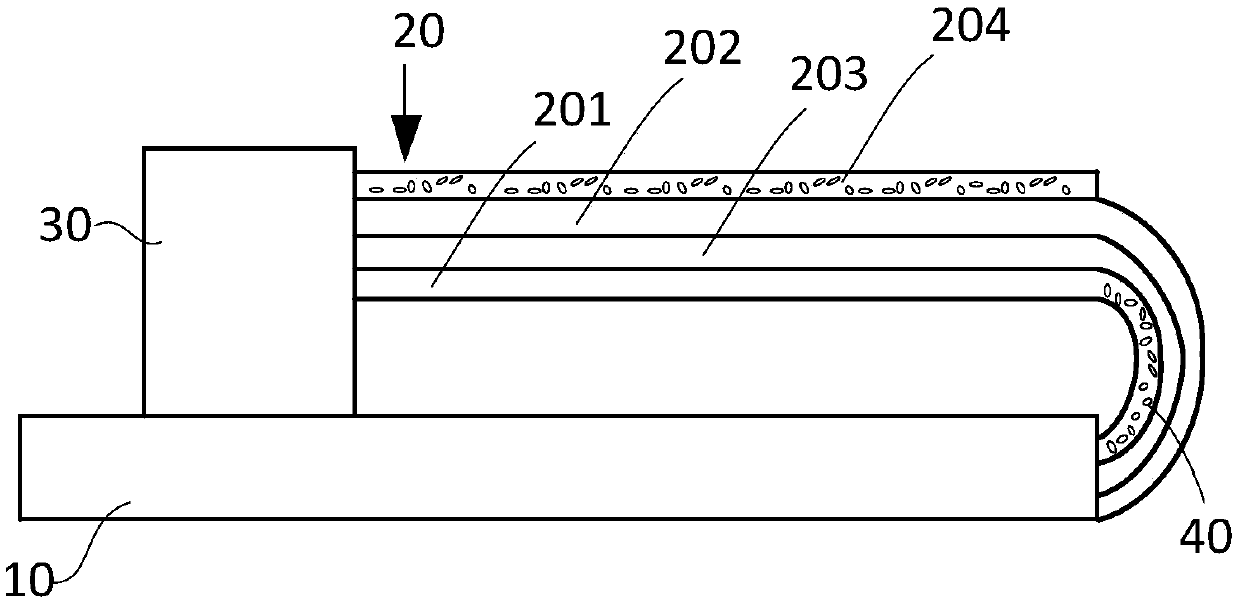
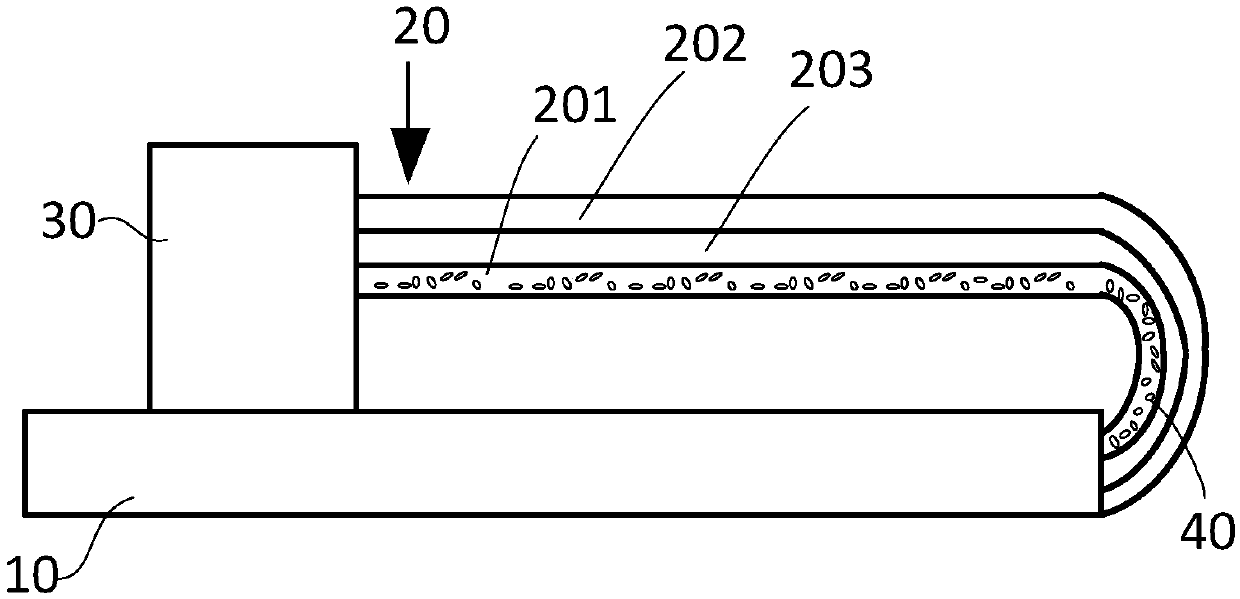
[0034] The present invention provides a display module and its manufacturing method and display device, which are used to provide a flexible circuit board. The flexible circuit board is provided with a wave-absorbing material, so that it is not necessary to attach an isolation electromagnetic material to the COF, so that the COF is relatively Thin, reducing the possibility of causing damage to the circuit.

[0035] The specific implementation manners of the display module provided by the embodiments of the present invention, its manufacturing method, and the display device will be described in detail below with reference to the accompanying drawings.

[0036] The thickness and sh...


PUM


Abstract

The invention discloses a display module, a manufacturing method of the display module, and a display device. A flexible circuit board is filled with a wave-absorbing material, thus an isolating electromagnetic material does not need to attach to a COF, so that the COF is thin, and thus the possibility of causing damage to the circuit is reduced. The display module comprises a display panel and the flexible circuit board connected with the display panel, and the flexible circuit board is provided with a bent area bent towards the back of the display panel; and the flexible circuit board is provided with a solder mask protection layer, and the wave-absorbing material is at least arranged in the solder mask protection layer of the bent area.

Description

technical field [0001] The invention relates to the technical field of displays, in particular to a display module, a manufacturing method thereof, and a display device. Background technique [0002] COF (Chip On Film, Chip On Film) is a chip soft film construction technology that fixes IC (Intergrated Circuit) on a flexible circuit board. The COF is usually bound in the binding area of ​​the display panel for driving the display device. [0003] However, based on the current demand for a narrow frame of the display device, the display panel Panel can be bent at its Pad end (the end connected to the external circuit), which causes the distance between the antenna in the display device and the COF to be relatively close, which will affect the COF Electromagnetic interference is caused, thereby causing the display of the display device to be affected. In order to reduce the electromagnetic interference caused by the antenna to the COF, a physical isolation method is currentl...

Claims


Application Information

Patent Timeline
IPC IPC(8): G09F9/00H05K1/02
CPCG09F9/00H05K1/0216
Inventor 李伟郭文峰曹雪颖李飞
Owner BOE TECH GRP CO LTD
Why Eureka
Try Eureka