

Wafer bonding device and wafer bonding method
A wafer bonding and wafer technology, applied in electrical components, semiconductor/solid-state device manufacturing, circuits, etc., can solve problems such as poor wafer bonding quality, improve performance, improve bonding effect, and increase alignment The effect of precision
- Summary
- Abstract
- Description
- Claims
- Application Information
AI Technical Summary
Problems solved by technology
Method used
Image

Examples
Embodiment Construction
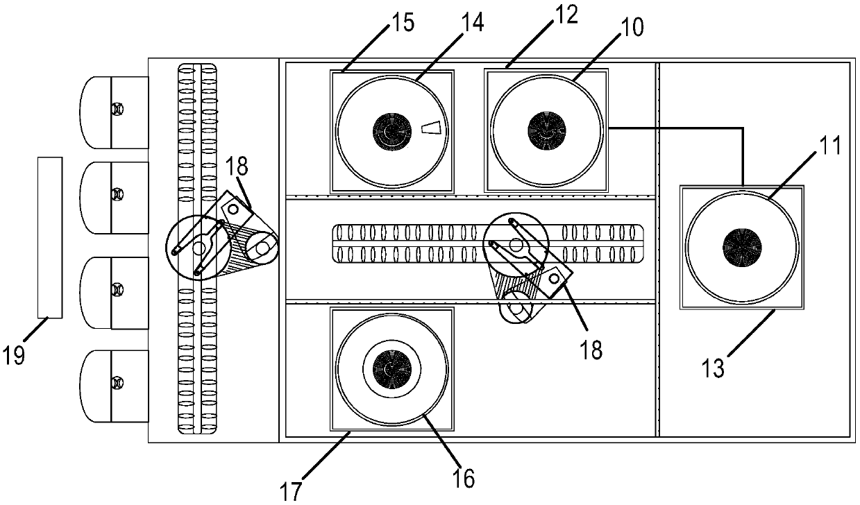
[0044] Specific implementations of the wafer bonding apparatus and wafer bonding method provided by the present invention will be described in detail below in conjunction with the accompanying drawings.
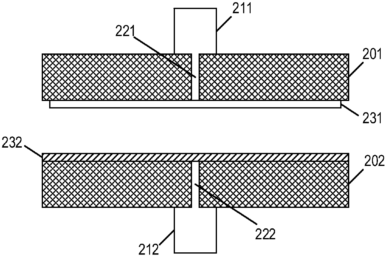
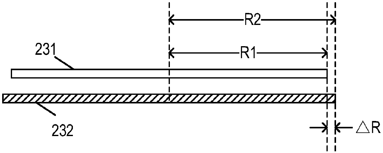
[0045] During the wafer bonding process, the alignment accuracy between two wafers to be bonded has a crucial impact on the final bonding quality. Due to the different manufacturing processes experienced by the two wafers before bonding, the two wafers will experience different degrees of three-dimensional expansion (Expansion), so in the actual bonding process, the dimensions of the two wafers are different. In general, the greater the difference in lateral dimensions between two wafers, the lower the alignment accuracy between the two wafers. However, the current wafer bonding process does not take into account the influence of the three-dimensional expansion of the two wafers to be bonded in the previous process on the size of the wafer during the bonding process, so that ...
PUM
 Abstract
Description
Claims
Application Information