Multi-chip simultaneous measurement structure and method

A multi-chip, chip technology, applied in the direction of measuring electricity, measuring devices, measuring electrical variables, etc., can solve the problems of excessive judgment and inability to test the power consumption parameters of a single DUT, so as to reduce misjudgments and increase the number of simultaneous measurements.

Active Publication Date: 2019-04-16
SHANGHAI HUAHONG GRACE SEMICON MFG CORP
View PDF7 Cites 4 Cited by
  • Summary
  • Abstract
  • Description
  • Claims
  • Application Information

AI Technical Summary

Problems solved by technology

[0005] In this way, although the number of simultaneous measurements has been increased, the disadvantages it brings are also obvious
First of all, due to the parallel structure, the test result is that the power consumption parameters of a single DUT cannot be tested, and only the total power consumption of a group of DUTs connected in parallel can be obtained; secondly, when these DUTs in a group of DUTs sharing a DPS resource channel When a DUT or some DUTs are short-circuited to the ground, the power of the entire group of DUTs can only be turned off, and all DUTs are set as invalid DUTs, so there is a situation of overkill, and in the periphery of the wafer, this situation will become obvious

Method used


Image

  • Multi-chip simultaneous measurement structure and method
  • Multi-chip simultaneous measurement structure and method
  • Multi-chip simultaneous measurement structure and method

Examples


Embodiment Construction

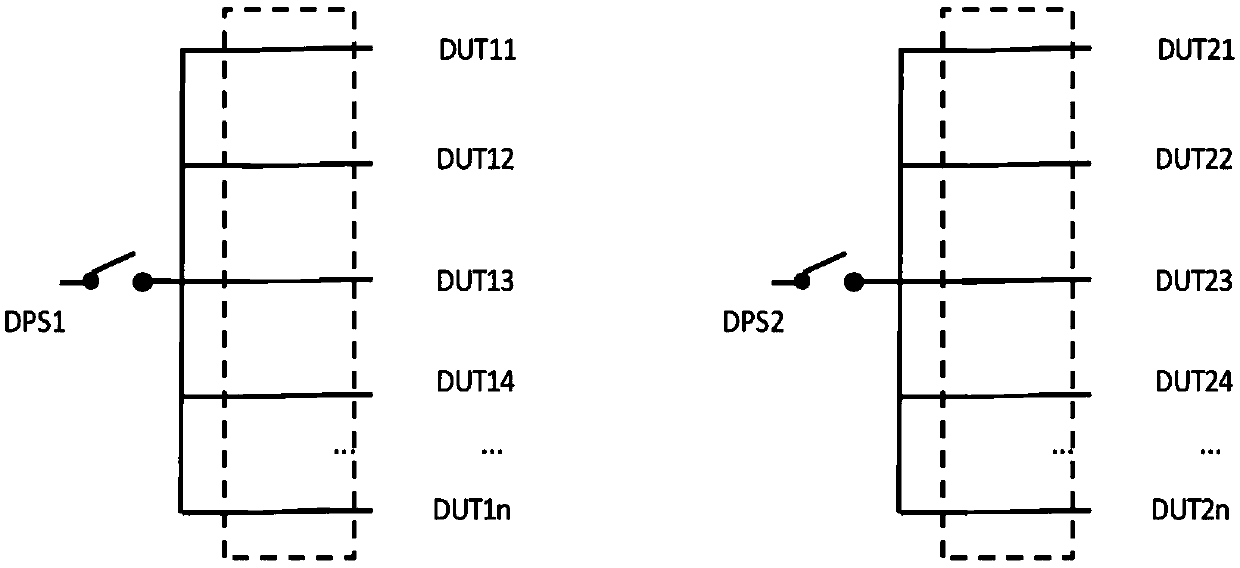
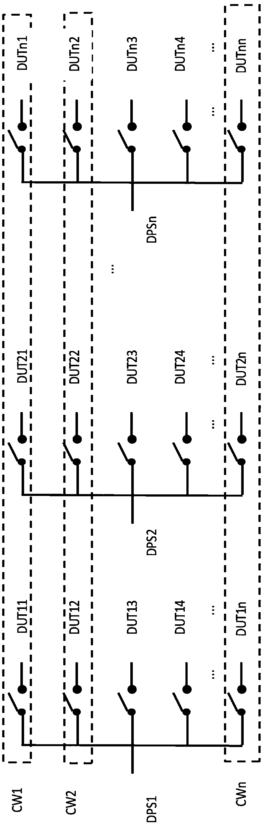
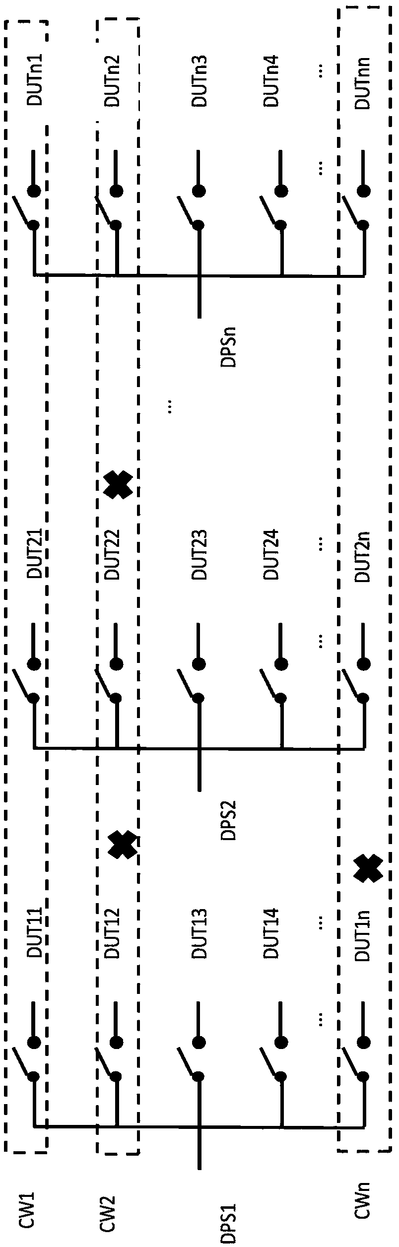
[0030] A kind of multi-chip simultaneous testing structure described in the present invention is for conducting electrical tests on the chips on the wafer, such as figure 2 As shown, the chip DUT to be tested on the wafer is divided into rows and columns to form a test array, and the chips to be tested on the same column are connected in parallel to form a test port of each column; the test port is connected to the power channel DPS of the tester, Contains DPS1~DPSn.

[0031] The chips to be tested on the same row share a control switch CW, from CW1 to CWn.

[0032] A tester, the tester has a plurality of power channels, one power channel of the tester corresponds to a row of test ports of the chips to be tested.

[0033] The chip to be tested includes a plurality of test pins; the number of rows of the test array is determined by the number of test pins of the chip to be tested, and the number of columns of the test array is determined by the number of power supply channels...


PUM


Abstract

The invention discloses a multi-chip simultaneous measurement structure. According to the multi-chip simultaneous measurement structure, an electrical test is performed on chips on a wafer; the chipsto be tested on the wafer are divided into rows and columns so as to form a test array, and the chips to be tested in the same column are connected in parallel so as to form the test port of each column; the test ports are connected with the power source channels of a tester; the chips to be tested on the same row share one control switch; and the tester is provided with a plurality of power source channels, and one power source channel of the tester is corresponding to the test port of the chips to be tested in one column. The invention also discloses a simultaneous measurement method of themulti-chip simultaneous measurement structure. According to the simultaneous measurement method of the multi-chip simultaneous measurement structure, the chips to be tested are reasonably matched withthe channels of the tester, and therefore, the number of chips that can be tested simultaneously can be increased, and the power consumption parameter test of each chip to be tested is realized; anda test unit that encounters a short circuit during test can be isolated by the corresponding control switch, and therefore, misjudgment can be reduced.

Description

technical field [0001] The invention relates to the field of manufacturing and testing of semiconductor integrated circuits, in particular to a method for simultaneously testing a plurality of chips (die) on a wafer. Background technique [0002] Chip testing is the measurement of electrical parameters on silicon wafer-level integrated circuits for the purpose of verifying acceptable electrical performance. The electrical specifications used during testing vary with the purpose of the test. [0003] In the semiconductor chip testing industry, with the continuous advancement of technology, the process size is getting smaller and smaller, and the chip area is getting smaller and smaller. In other words, the number of chips (die) on the same size wafer is increasing . For wafer testing, due to the increase in the number of chips, if the same test number remains unchanged, the test efficiency will inevitably decrease. Since the testing process does not increase the value of t...

Claims


Application Information

Patent Timeline
Patent Type & Authority Applications(China)
IPC IPC(8): G01R31/28H01L21/66
CPCG01R31/2851G01R31/2853H01L22/14H01L22/34
Inventor 谢晋春辛吉升
Owner SHANGHAI HUAHONG GRACE SEMICON MFG CORP
Why Eureka
Try Eureka