Array substrate, display panel and display device

A technology for array substrates and display areas, which is applied in the direction of instruments, semiconductor devices, electrical components, etc., and can solve problems such as large thickness of protective layer, inability to realize electrical connection between gold fingers and bonding pads, insufficient deformation of conductive particles, etc.

Inactive Publication Date: 2019-04-19
EVERDISPLAY OPTRONICS (SHANGHAI) CO LTD
View PDF6 Cites 26 Cited by
  • Summary
  • Abstract
  • Description
  • Claims
  • Application Information

AI Technical Summary

Problems solved by technology

However, the protective layer in the prior art is usually formed by a passivation layer with a thickness of 1.5 μm to 2 μm. When the anisotropic conductive adhesive including conductive particles is used to realize the electrical connection between the bonding pad and the gold finger, if there is an alignment Deviation, after the conductive particles between the gold finger and the protective layer reach the maximum deformation, the gold finger cannot be pressed down further, because the bonding pad is set on the side of the protective layer close to the substrate, and the thickness of the protective layer is relatively large, resulting in The distance between the gold finger and the bonding pad is much greater than the distance between the gold finger and the protective layer, so that the deformation of the conductive particles between the gold finger and the bonding pad is insufficient, and the electrical connection between the gold finger and the bonding pad cannot be realized

Method used


Image

  • Array substrate, display panel and display device
  • Array substrate, display panel and display device
  • Array substrate, display panel and display device

Examples


Embodiment Construction

[0020] In order to further explain the technical means and effects of the present invention to achieve the intended purpose of the invention, the specific implementation, structure, Features and their functions are described in detail below.

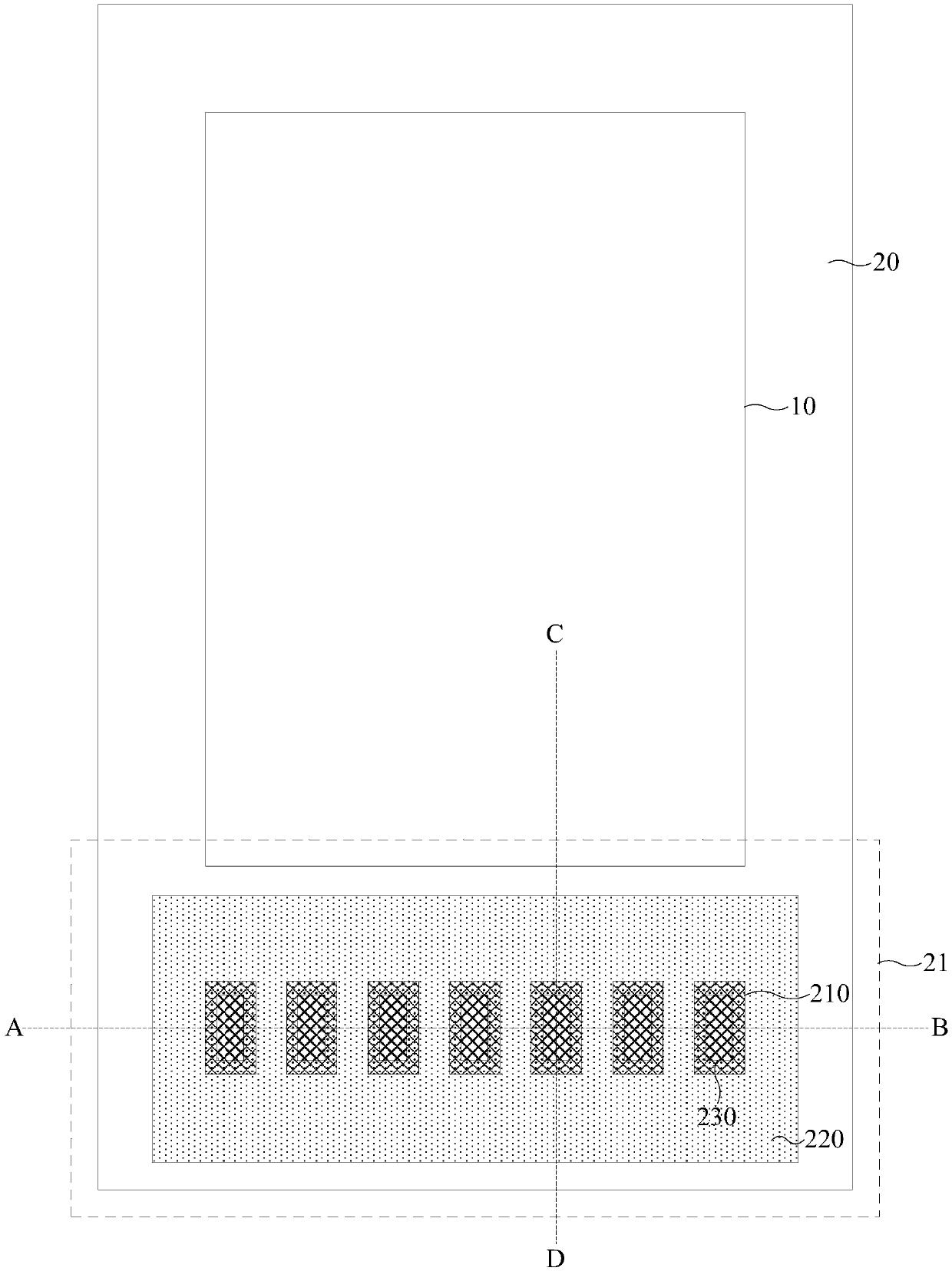
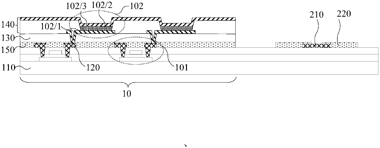
[0021] An embodiment of the present invention provides an array substrate, and the array substrate includes a display area and a non-display area arranged around the display area;

[0022] The non-display area includes a binding area located on one side of the display area, and the binding area is provided with a plurality of binding pads;

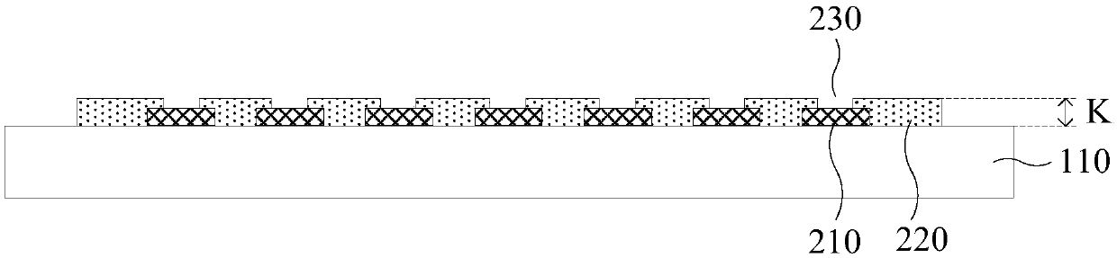
[0023] The array substrate includes a substrate, and a protective layer is formed on a side of the bonding pad away from the substrate, and the protective layer includes a plurality of openings, and the openings are connected to the bonding pad one by one. Correspondingly, the opening penetrates the protective layer to expose a part of the surface corresponding to the bonding pad;

[0024] The thic...


PUM

PropertyMeasurementUnit
diameteraaaaaaaaaa
thicknessaaaaaaaaaa
thicknessaaaaaaaaaa

Abstract

The invention discloses an array substrate, a display panel and a display device. The array substrate includes a display area and a non-display area disposed around the display area; the non-display area includes a binding area arranged at one side of the display area, and the binding area is provided with a plurality of binding pads; the array substrate comprises a substrate, a protection layer is arranged at one sides, far away from the substrate, of the binding pads, the protection layer comprises a plurality openings which are in one-to-one correspondence with the binding pads, and the openings penetrate the partial surfaces, where the binding pads are exposed, of the protection layer; and the thickness value of the protection layer is in a range of 0.3-0.6[Mu]m. According to the technical scheme provided by the embodiment, when the flexible printed circuit board and the array substrate are subjected to alignment deviation, a gold finger and conducting particles between the corresponding binding pads still can generate effective deformation to achieve electrical connection of the gold finger and the corresponding binding pads.

Description

technical field [0001] Embodiments of the present invention relate to the binding technology of flexible printed circuit boards, and in particular to an array substrate, a display panel and a display device. Background technique [0002] With the continuous advancement of display technology, display panels are applied to various electronic devices. [0003] The display panel includes a driving circuit, which can provide driving signals to realize the normal display of images. Usually, the driving circuit is formed on a flexible printed circuit board, and then the flexible printed circuit board is bound to the array substrate in the display panel. Since the flexible printed circuit board can be bent to the side of the array substrate away from the light-emitting surface of the display panel, the non-display area of ​​the display panel will not be widened by the flexible printed circuit board. The array substrate is provided with a plurality of binding pads, and the flexible ...

Claims


Application Information

Patent Timeline
Patent Type & Authority Applications(China)
IPC IPC(8): H01L27/02G02F1/1362
CPCG02F1/1362H01L27/0207
Inventor 施凯挺
Owner EVERDISPLAY OPTRONICS (SHANGHAI) CO LTD
Why Eureka
Try Eureka