Array substrate, display panel, and display device
A technology for array substrates and display devices, which is applied to electrical components, electric solid state devices, circuits, etc., can solve the problems of insufficient charging of pixel electrodes and distortion of display panel display images.
- Summary
- Abstract
- Description
- Claims
- Application Information
AI Technical Summary
Problems solved by technology
Method used
Image

Examples
Embodiment Construction
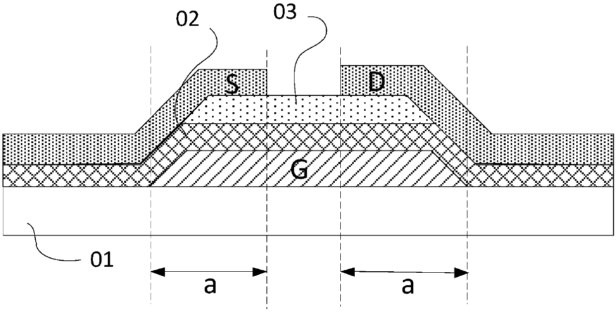
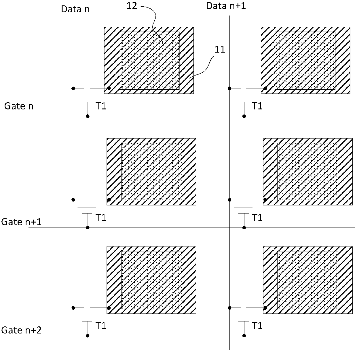
[0029] The inventors found that in the related art, such as figure 1 and figure 2 As shown, the array substrate includes a plurality of pixel regions arranged in an array, each pixel region includes a pixel electrode 11, a common electrode 12 and a first transistor T1, the gate G of the first transistor T1 is connected to the gate line Gate, and the first transistor T1 The source electrode S of T1 is connected to the pixel electrode 11, the drain electrode D of the first transistor T1 is connected to the data line Data, the orthographic projection of the common electrode 12 on the base substrate 01 and the orthographic projection of the pixel electrode 11 on the base substrate 01 There is an overlapping area a, and the common electrode 12 is loaded with a fixed voltage signal, that is, the common voltage signal VCOM. Since the gate G of the first transistor T1 has an overlapping area a with the source electrode S and the drain electrode D, the source electrode S and the gate...
PUM
 Abstract
Description
Claims
Application Information
 - R&D
- Intellectual Property
- Life Sciences
- Materials
- Tech Scout
- Unparalleled Data Quality
- Higher Quality Content
- 60% Fewer Hallucinations
Browse by: Latest US Patents, China's latest patents, Technical Efficacy Thesaurus, Application Domain, Technology Topic, Popular Technical Reports.
© 2025 PatSnap. All rights reserved.Legal|Privacy policy|Modern Slavery Act Transparency Statement|Sitemap|About US| Contact US: help@patsnap.com