GaN-based light-emitting diode epitaxial wafer and preparation method thereof

A technology of light-emitting diodes and epitaxial wafers, which is applied to electrical components, circuits, semiconductor devices, etc., can solve the problems of poor wavelength uniformity of epitaxial wafers and large warpage of epitaxial wafers, so as to improve wavelength uniformity and reduce voltage The effect of stress

Active Publication Date: 2019-04-23
HC SEMITEK ZHEJIANG CO LTD
View PDF13 Cites 1 Cited by
  • Summary
  • Abstract
  • Description
  • Claims
  • Application Information

AI Technical Summary

Problems solved by technology

[0003] In the process of realizing the present invention, the inventors have found that the prior art has at least the following problems: when the buffer layer is an AlN buffer layer, there is a relatively large compressive stress between the AlN and GaN, which will cause large warping of the epitaxial wafer. Curvature, the wavelength of the epitaxial wafer manifests as a bulge in the center and diffuses to the edge of the epitaxial wafer in the form of concentric circles, resulting in poor wavelength uniformity of the epitaxial wafer

Method used


Image

  • GaN-based light-emitting diode epitaxial wafer and preparation method thereof
  • GaN-based light-emitting diode epitaxial wafer and preparation method thereof
  • GaN-based light-emitting diode epitaxial wafer and preparation method thereof

Examples


Embodiment Construction

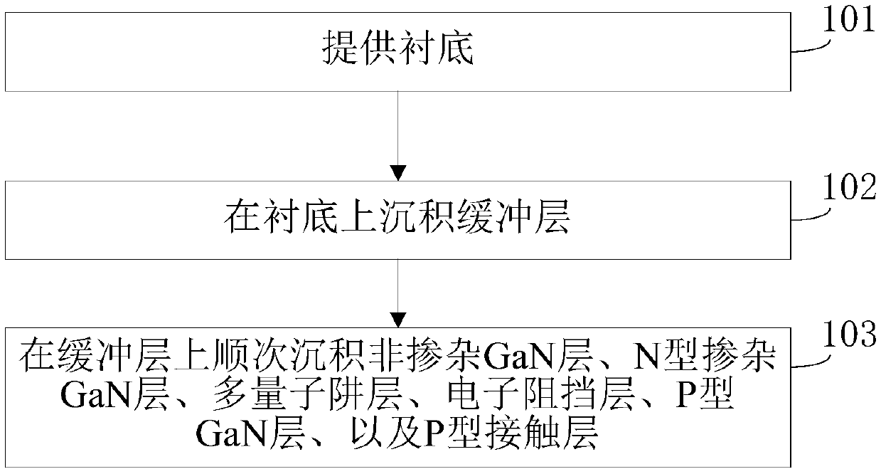
[0030] In order to make the object, technical solution and advantages of the present invention clearer, the implementation manner of the present invention will be further described in detail below in conjunction with the accompanying drawings.

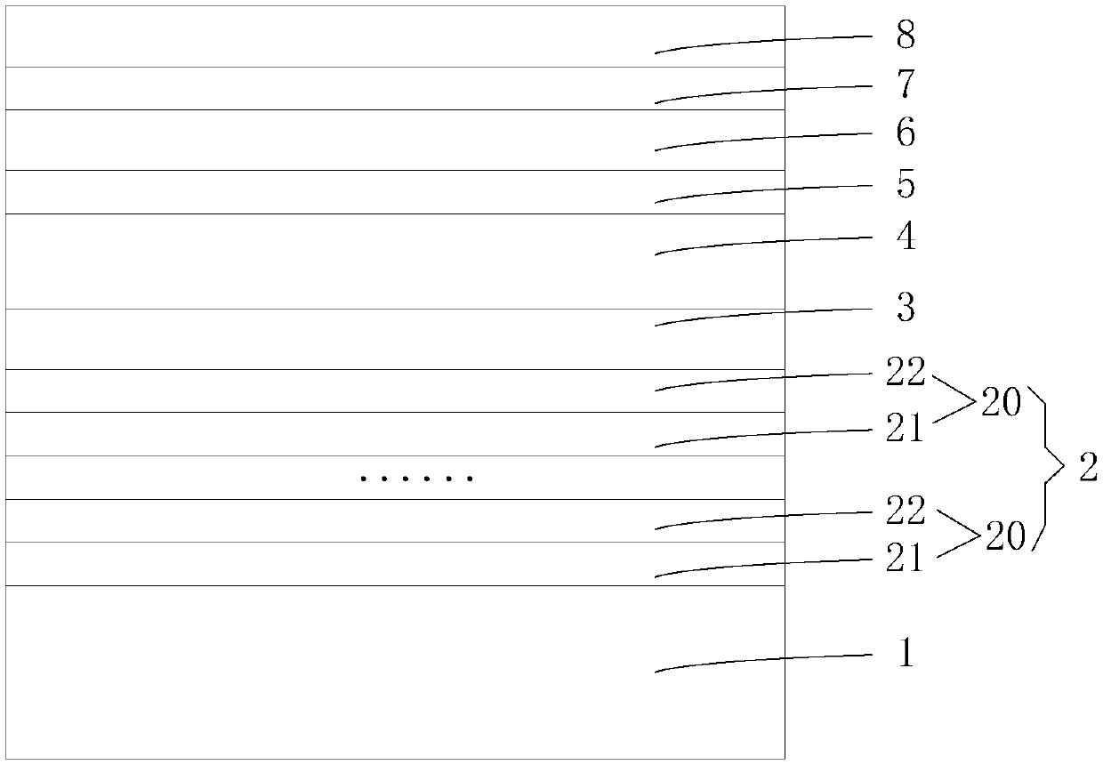
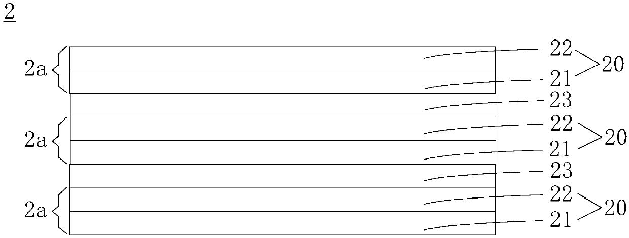
[0031] figure 1 A GaN-based light-emitting diode epitaxial wafer provided by an embodiment of the present invention is shown. see figure 1 , the light-emitting diode epitaxial wafer includes: a substrate 1, and a buffer layer 2 deposited sequentially on the substrate 1, an undoped GaN layer 3, an N-type doped GaN layer 4, a multi-quantum well layer 5, and an electron blocking layer 6. P-type GaN layer 7 and P-type contact layer 8 . Wherein, the buffer layer 2 includes several laminated composite layers 20 . The composite layer 20 includes an AlN sublayer 21 and an AlNO sublayer 22 , and the oxygen content of the AlNO sublayer 21 in each composite layer 20 increases from the composite layer 20 closest to the substrate 1 to the compos...


PUM

PropertyMeasurementUnit
thicknessaaaaaaaaaa
thicknessaaaaaaaaaa
thicknessaaaaaaaaaa

Abstract

The invention discloses a GaN-based light-emitting diode epitaxial wafer and a preparation method thereof, and belongs to the field of GaN-based light-emitting diodes. The method includes the steps of: providing a substrate; depositing a buffer layer on the substrate, the buffer layer comprising a plurality of stacked composite layers, each composite layer comprising an AlN sub-layer and an AlNO sub-layer, the oxygen content of the AlNO sub layer in each composite layer is gradually increased from a composite layer being closet to the substrate to a composite layer being farthest to the substrate; and depositing an undoped GaN layer, an N-doped GaN layer, a quantum well layer, an electron blocking layer, a P-type GaN layer and a P-type contact layer on the buffer layer in order.

Description

technical field [0001] The invention relates to the field of GaN-based light-emitting diodes, in particular to a GaN-based light-emitting diode epitaxial wafer and a preparation method thereof. Background technique [0002] A GaN (gallium nitride)-based LED (Light Emitting Diode, light emitting diode) generally includes an epitaxial wafer and electrodes prepared on the epitaxial wafer. The epitaxial wafer usually includes: a substrate, and a GaN-based epitaxial layer grown on the substrate. The epitaxial layer includes a sequentially stacked buffer layer, a non-doped GaN layer, an N-type GaN layer, and an MQW (Multiple Quantum Well, multiple quantum well ) layer, electron blocking layer, P-type GaN layer and contact layer. When a current is injected into the GaN-based LED, the electrons in the N-type region such as the N-type GaN layer and the holes in the P-type region such as the P-type GaN layer enter the MQW active region and recombine to emit visible light. Wherein, t...

Claims


Application Information

Patent Timeline
Patent Type & Authority Applications(China)
IPC IPC(8): H01L33/12H01L33/00
CPCH01L33/0066H01L33/0075H01L33/12
Inventor 刘旺平张武斌乔楠胡加辉李鹏
Owner HC SEMITEK ZHEJIANG CO LTD
Why Eureka
Try Eureka