Two-dimensional scanning varactor active super-surface electromagnetic lens antenna
A two-dimensional scanning, electromagnetic lens technology, applied in the field of millimeter wave and terahertz communication, can solve the problems of increasing the number of bias lines and too many bias lines in the lens
- Summary
- Abstract
- Description
- Claims
- Application Information
AI Technical Summary
Problems solved by technology
Method used
Image
Examples
Embodiment 1
[0039] A two-dimensional scanning varactor active metasurface electromagnetic lens antenna provided in this embodiment includes a focusing lens 1, a two-dimensional scanning array 2, a spacer 3, a support column 4, a horn antenna 5 and a base 6; The lens 1 is a metasurface electromagnetic lens, and the two-dimensional scanning array 2 is a metasurface; the two-dimensional scanning array 2, the focusing lens 1, and the support column 4 are all sequentially connected by a gasket 3, and the support column 4 is fixed on the base 6, the horn antenna 5 is fixed on the base 6, and the horn mouth of the horn antenna 5 faces the focusing lens 1; the two-dimensional scanning array 2 consists of two one-dimensional scanning arrays: x direction scanning array 7 and y direction The scanning array 8 is superimposed in the z direction, the y direction is used as the polarization direction, the z direction is used as the lens symmetry axis direction, and the bias line directions of the varacto...
Embodiment 2
[0051] In a preferred embodiment of the present invention, the two-dimensional scanning varactor active metasurface electromagnetic lens antenna works in the Ka frequency band.
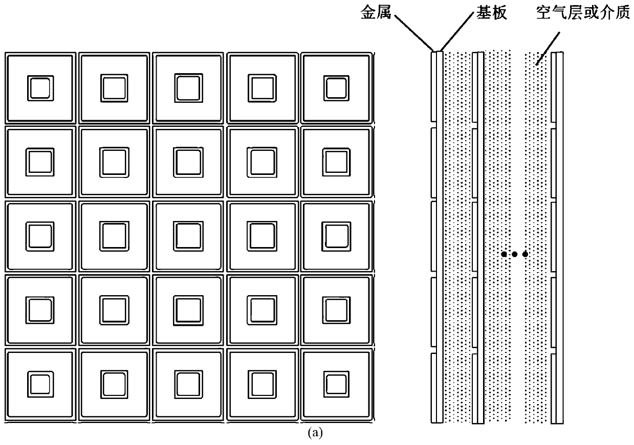
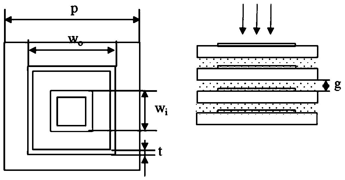
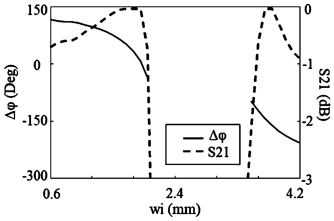
[0052] refer to figure 1 with figure 2 as shown, figure 1 It is a schematic diagram of the metasurface structure of the focusing lens 1 in the preferred embodiment of the present invention; figure 2 It is a schematic diagram of the structural dimensions of the metasurface unit of the focusing lens 1 in the preferred embodiment of the present invention. The focusing lens 1 adopts a four-layer metasurface structure, and each layer is composed of periodically arranged units. The unit adopts a double-square ring structure, and a metal square ring with a width of t is etched on the printed medium board with a period of p, and the inner ring has a side length of w i , the outer ring side length w o , the interlayer spacing g, while maintaining the size of the outer ring, adjust the phase shift of pas...
PUM
 Abstract
Description
Claims
Application Information


