A method to optimize usb link impedance

A link and connector technology, which is applied in the improvement field of motherboard signal transmission lines, can solve problems such as impedance discontinuity, affecting signal transmission quality, and insufficient optimization of USB link impedance, so as to ensure uniformity and improve link impedance consistency Sex, to avoid the effect of falling first and then rising

Active Publication Date: 2020-07-28
INSPUR SUZHOU INTELLIGENT TECH CO LTD
View PDF5 Cites 0 Cited by
  • Summary
  • Abstract
  • Description
  • Claims
  • Application Information

AI Technical Summary

Problems solved by technology

[0007] Although this measure can reduce impedance discontinuity to a certain extent and ensure local impedance continuity, since the entire USB link will have Cable, front control board and other parts in addition to the motherboard, the impedance of these parts and the motherboard wiring Impedances are not necessarily the same, which leads to the phenomenon that the local impedance of the USB link is consistent but the overall impedance is still discontinuous, which will also affect the quality of signal transmission
In this regard, most of the prior art optimizes the USB link by reducing the link impedance, but this leads to insufficient overall impedance optimization of the USB link, which is also a problem that needs to be solved urgently in this field.

Method used


Image

  • A method to optimize usb link impedance
  • A method to optimize usb link impedance
  • A method to optimize usb link impedance

Examples


Embodiment Construction

[0024] In order to make the purpose, technical solutions and advantages of the embodiments of the present invention clearer, the technical solutions in the embodiments of the present invention will be clearly and completely described below in conjunction with the drawings in the embodiments of the present invention. Obviously, the described embodiments It is a part of embodiments of the present invention, but not all embodiments.

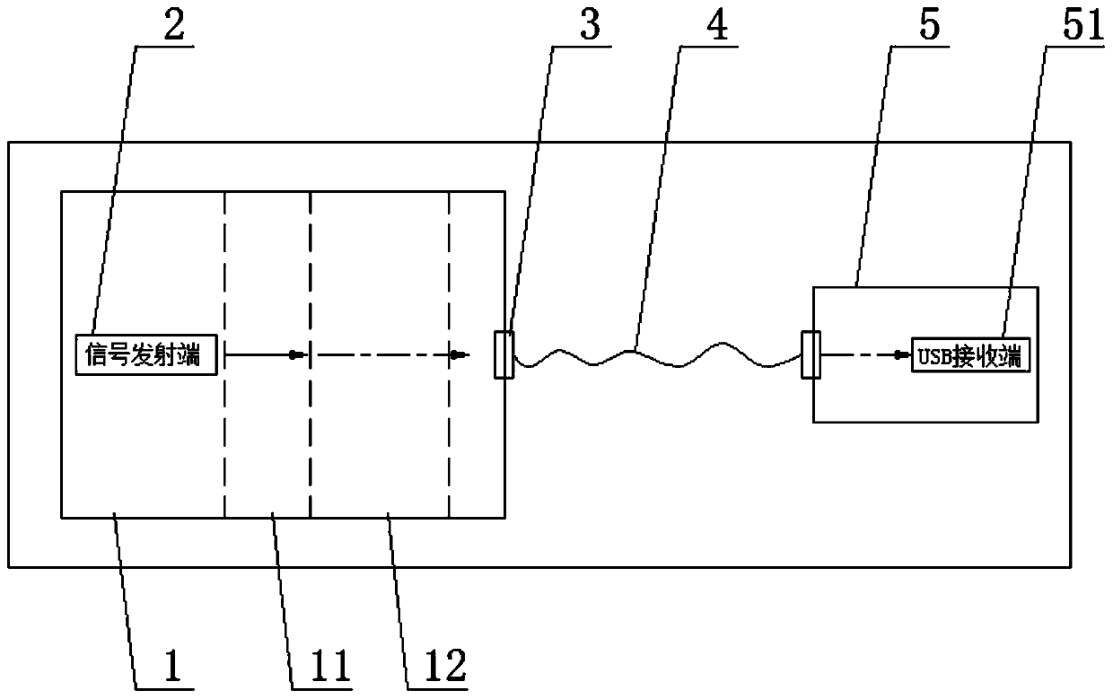
[0025] Such as Figure 1-Figure 3 As shown, a method for optimizing the impedance of a USB link disclosed in this embodiment includes a motherboard 1 equipped with a signal transmitting end 2, a connector 3, and a USB cable for signal transmission between an external USB device 5 and the connector 3 The cable 4, the signal transmitting end 2, the connector 3, and the USB cable 4 are electrically connected in sequence to form a USB signal transmission link, and the impedance optimization method of the USB signal transmission link is realized through ...


PUM


Abstract

The invention relates to a method for optimizing USB link impedance. The method for optimizing the USB link impedance comprises a main board and a USB cable, wherein a signal emitting end and a connector are installed on the main board, and a USB signal transmission link is formed beteewn the signal emitting end, the connector and the USB cable in sequence. The USB signal transmission link impedance optimization method is realized by the following steps that S1, the USB signal transmission link from the signal emitting end of the main board to the connector is divided into a BGA area and a normal routing area according to the layout distribution of the main board, wherein the USB link impedance in the normal routing area and in the BGA area are the same; and S2, the USB link impedance of the USB signal transmission link between the connector of the main board and the USB cable is set the same as in the BGA area or the normal routing area. Contrary to common impedance optimization measures adopted in the prior art, the method for optimizing the USB link impedance ensures the unity of the overall link impedance by increasing the USB link impedance in normal area routing area and obtains better effects.

Description

technical field [0001] The invention relates to the improvement of the signal transmission line of the motherboard, in particular to a method for optimizing the impedance of the USB link. Background technique [0002] The full name of USB (Universal Serial Bus) is Universal Serial Bus, which is used to standardize the connection and communication between the host computer and external devices. USB is an interface technology used in the field of PC and electronic communication. It supports plug-and-play and hot-swappable functions of devices. Because of its strong data transmission signal and wide application range, it is widely used in various electronic devices. [0003] The USB device system is divided into two parts, the USB Host end and the USB Device end. Taking the U disk with the USB interface as an example, the U disk itself is a USB Device, and the USB interface of the PC and related control circuits are the USB Host part. Each part is composed of a hardware part a...

Claims


Application Information

Patent Timeline
Patent Type & Authority Patents(China)
IPC IPC(8): H05K1/02G06F13/42
Inventor 荣世立刘法志
Owner INSPUR SUZHOU INTELLIGENT TECH CO LTD
Why Eureka
Try Eureka