Optical Fingerprint Recognition Device

A fingerprint identification and optical technology, applied in the field of fingerprint identification, can solve the problems of light refraction and scattering, affect the clarity of fingerprint imaging, and affect the reliability of fingerprint identification, etc., to achieve the effect of improving signal-to-noise, improving clarity, and improving reliability

Active Publication Date: 2021-04-02
WUHAN CHINA STAR OPTOELECTRONICS TECH CO LTD
View PDF11 Cites 0 Cited by
  • Summary
  • Abstract
  • Description
  • Claims
  • Application Information

AI Technical Summary

Problems solved by technology

[0004] The present invention provides an optical fingerprint identification device to solve the existing optical fingerprint identification module. Since the light used for fingerprint identification needs to pass through different media during the transmission process, the reflected light will be refracted and scattered, and then Issues that affect the clarity of fingerprint imaging on the optical fingerprint chip, which in turn affects the reliability of fingerprint recognition

Method used


Image

  • Optical Fingerprint Recognition Device
  • Optical Fingerprint Recognition Device
  • Optical Fingerprint Recognition Device

Examples


Embodiment 1

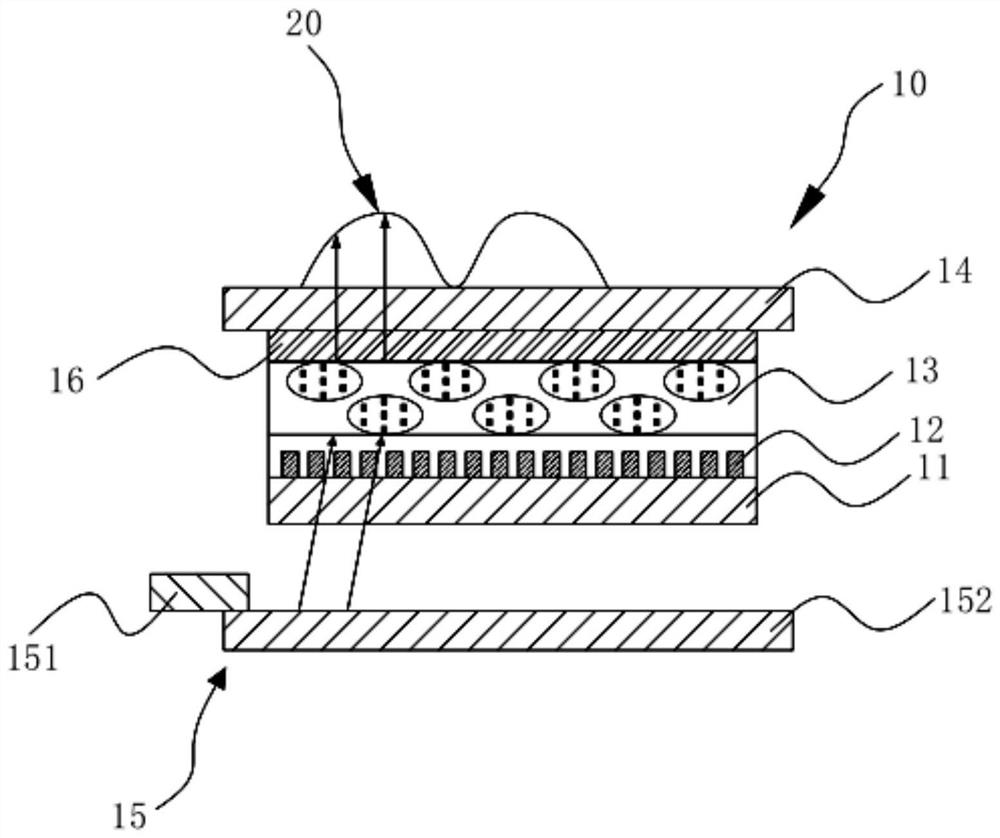
[0025] like figure 1 As shown, the present invention provides an optical fingerprint identification device 10 , which includes a substrate 11 , a photosensitive element 12 , a collimation layer 13 , a cover plate 14 , and a backlight module 15 .

[0026] The photosensitive element 12 is disposed on the substrate 11 , the cover plate 14 is disposed on the photosensitive element 12 , and the cover plate 14 is located on the top layer of the fingerprint identification device 10 for encapsulation and protection. For the function of the device, the cover plate 14 is made of transparent glass, and the cover plate 14 is in contact with the human fingerprint 20 .

[0027] The backlight module 15 is disposed on the side of the substrate 11 away from the photosensitive element 12 , and the backlight module 15 provides a light source for optical fingerprint recognition.

[0028] The alignment layer 13 is formed by dispersing liquid crystals in a solid organic polymer. The material of th...

Embodiment 2

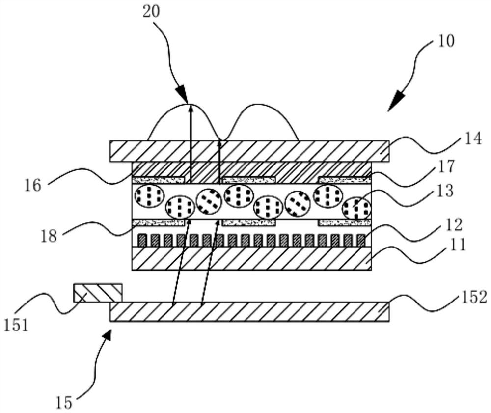
[0039] like figure 2 As shown, the difference from the first embodiment is that the two opposite surfaces of the alignment layer 13 are respectively provided with a first electrode layer 17 and a second electrode layer 18, and the first electrode layer 17 is provided on the alignment layer 13 is on a side surface (upper surface) facing away from the substrate 11 , and the second electrode layer 18 is disposed on a side surface (lower surface) of the alignment layer 13 close to the substrate 11 . The electrode patterns of the first electrode layer 17 and the second electrode layer 18 are the same and correspondingly arranged. The materials of the first electrode layer 17 and the second electrode layer 18 are ITO (Indium tin oxide, indium oxide). tin).

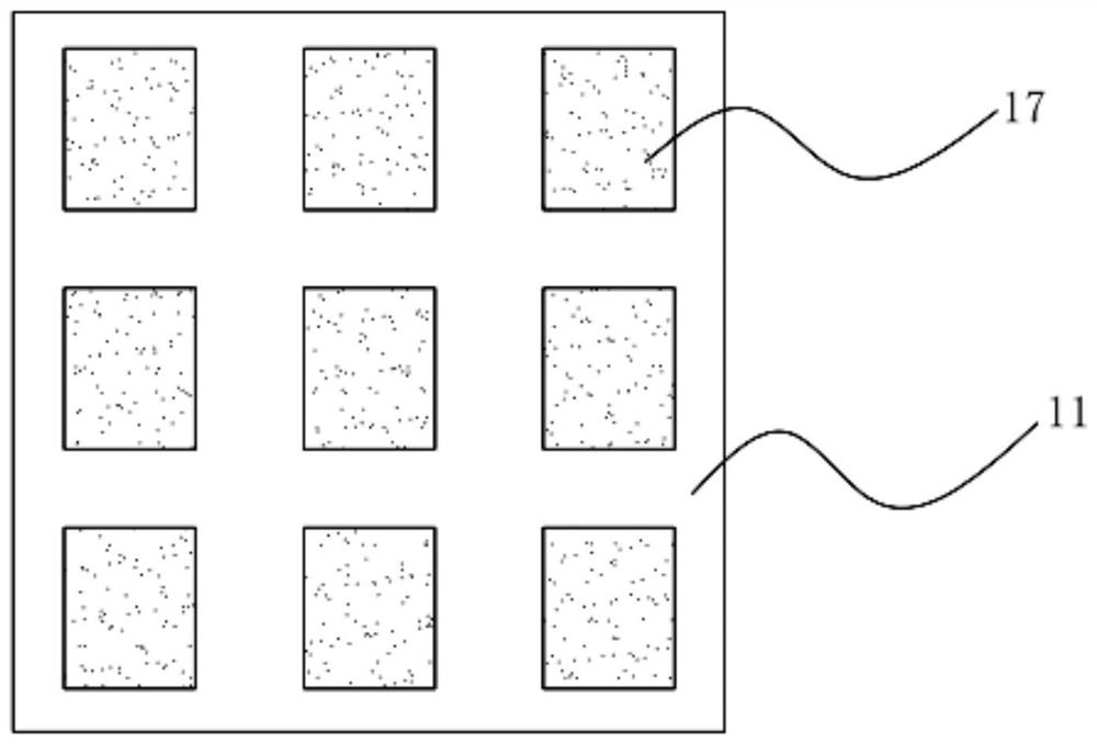
[0040] like image 3 As shown, the electrode patterns of the first electrode layer 17 are electrode small blocks distributed in an array, the length and width of the electrode small blocks can be 2-100 microns, and the row sp...

Embodiment 3

[0043] like Figure 4 As shown, this embodiment provides an optical fingerprint identification device 30 , which includes a substrate 31 , a photosensitive element 32 , an alignment layer 33 , an OLED display layer 35 , an adhesive layer 36 , and a cover plate 34 .

[0044] The photosensitive element 33 is disposed on the substrate 31, the collimation layer 33 is disposed on the photosensitive element 32, the cover plate 34 is disposed on the collimation layer 33, and the OLED display The layer 35 is disposed between the alignment layer 33 and the cover plate 34 .

[0045] The adhesive layer 36 is disposed on the cover plate 34 and the OLED display layer 35 for adhering the cover plate 34 and the OLED display layer 35 .

[0046] The substrate 31 can be a flexible substrate, and the cover plate 34 is transparent glass, which is used to encapsulate and protect the device, and is in contact with the human fingerprint 20 .

[0047] The alignment layer 35 is a PDLC film, the refr...


PUM

PropertyMeasurementUnit
thicknessaaaaaaaaaa
widthaaaaaaaaaa
transmittivityaaaaaaaaaa

Abstract

An optical fingerprint identification device, including a substrate, a photosensitive element, a cover plate, and an alignment layer arranged between the cover plate and the substrate, the alignment layer is composed of liquid crystal dispersed in a solid organic polymer formed in. By setting the collimation layer made of polymer dispersed liquid crystal, the signal to noise can be improved, and the definition of fingerprints on the photosensitive element can be improved; in addition, compared with the existing lens, the full-surface collimation layer has the ability to avoid collision And relative displacement and other advantages can improve the reliability of fingerprint recognition.

Description

technical field [0001] The invention relates to the technical field of fingerprint identification, in particular to an optical fingerprint identification device. Background technique [0002] With the continuous development of technology, the screen ratio of mobile terminals such as mobile phones is getting higher and higher, and full-screen mobile terminals have become a development trend. For fingerprint recognition of full-screen mobile terminals, conventional capacitive fingerprints cannot penetrate cover glass with a thickness of more than 0.5 mm, so they are no longer suitable for the development trend of full-screen mobile terminals, but optical fingerprints with good penetration. has become a new technological direction. [0003] At present, for the full-screen optical fingerprint recognition design, the optical fingerprint recognition module is generally placed below the display area. The light used for fingerprint recognition needs to pass through the glass cover...

Claims


Application Information

Patent Timeline
Patent Type & Authority Patents(China)
IPC IPC(8): G06K9/00G02F1/1334
CPCG02F1/1334G06F18/00
Inventor 刘凡成何剑
Owner WUHAN CHINA STAR OPTOELECTRONICS TECH CO LTD
Why Eureka
Try Eureka