A silicon carbide trench Schottky diode device and its preparation method

A Schottky diode, silicon carbide technology, applied in semiconductor/solid-state device manufacturing, semiconductor devices, electrical components, etc., can solve the problem of inability to improve surge current resistance, achieve low specific on-resistance, reduce forward Effects of voltage drop, high surge current capability

Active Publication Date: 2020-09-15
HUNAN SANAN SEMICON CO LTD
View PDF8 Cites 0 Cited by
  • Summary
  • Abstract
  • Description
  • Claims
  • Application Information

AI Technical Summary

Problems solved by technology

For the TMBS structure, since there is no P-type injection region, the ability to resist surge current cannot be improved through the conductance modulation effect.

Method used


Image

  • A silicon carbide trench Schottky diode device and its preparation method
  • A silicon carbide trench Schottky diode device and its preparation method
  • A silicon carbide trench Schottky diode device and its preparation method

Examples


Embodiment 1

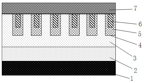
[0069] like image 3 As shown, a silicon carbide trench Schottky diode device includes from bottom to top: cathode electrode 1, substrate layer 2, N-type SiC epitaxial layer 3, trench 4, dielectric layer 5, conductive layer 6 and anode electrode 7 , a plurality of trenches 4 are located on the top of the N-type SiC epitaxial layer 3, the dielectric layer 5 and the conductive layer 6 are filled in the trenches 4 in sequence, and a P-type region 8 is also included, and the P-type region 8 is embedded in part of the trenches 4 between the N-type SiC epitaxial layer 3 and the junction of the anode electrode 7, the P-type region 8 is located in the N-type SiC epitaxial layer 3, and the upper boundary 81 of the P-type region 8 is connected to the anode electrode 7, and the P-type region 8 The side boundary 83 borders on the side wall 43 of the trench 4 , and the side boundary 83 is a boundary parallel to the side wall 43 of the trench 4 .

[0070] Present embodiment is prepared by ...

Embodiment 2

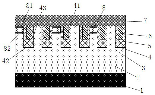
[0077] like Figure 4 As shown, the upper boundary 81 of the P-type region 8 protrudes above the trench 4 and is connected to the anode electrode 7 , and the lower boundary 82 is located on or above the top 41 of the trench 4 . This structure allows the P-type region 8 to be directly formed by epitaxial growth, avoiding material damage caused by ion implantation and activation processes, and also simplifies the process.

[0078] In another embodiment of the present invention, the dielectric layer 5 extends upward from the lower boundary 82 of the P-type region 8 to the side boundary of the P-type region, may extend to the upper boundary 81 of the P-type region 8, and may not extend to the P-type region. The upper boundary 81 of the area 8 is set according to actual needs. In this way, the connection between the anode electrode 7 and the N-type SiC epitaxial layer 3 can be avoided, and the short circuit between the P-type region 8 and the N-type SiC epitaxial layer 3 can preve...

Embodiment 3

[0087] like Figure 5 As shown, the difference from the first embodiment is that the side boundary 83 of the P-type region 8 does not border on the sidewall 43 of the trench 4 . And its preparation method is the same.


PUM


Abstract

Disclosed is a SiC trench Schottky diode device, comprising, from bottom to top, a cathode electrode, a substrate layer, an N-type SiC epitaxial layer, trenches, a dielectric layer, a conductive layer, and an anode electrode, wherein the plurality of trenches are located on top of the N-type SiC epitaxial layer, and the dielectric layer and the conductive layer are sequentially filled in the trenches. The SiC trench Schottky diode device further comprises a P-type region embedded between some of the trenches and located at where the N-type SiC epitaxial layer and the anode electrode are connected. The invention increases the density of forward currents of the device, and improves the surge withstand capability of the device.

Description

technical field [0001] The invention belongs to the manufacturing process of semiconductor devices, in particular to a silicon carbide trench Schottky diode device and a preparation method thereof. Background technique [0002] Silicon carbide (SiC) has a series of excellent material properties such as high band gap, high thermal conductivity, high critical breakdown electric field strength, high electron mobility, etc., which meets the needs of future power electronic devices in high temperature, high frequency, high power and To meet the requirements of anti-harsh environment and other aspects, its industrialization process has attracted much attention. Since commercialization began in 2001, SiC Schottky diodes have been widely used in the market, and SiC Schottky diodes from many manufacturers have been updated and iterated many times. [0003] At this stage, the mainstream SiC Schottky diode structure on the market is the JBS / MPS structure, such as figure 1 As shown, t...

Claims


Application Information

Patent Timeline
Patent Type & Authority Patents(China)
IPC IPC(8): H01L29/06H01L21/329H01L21/266H01L29/872
CPCH01L21/266H01L29/06H01L29/872
Inventor 刘胜北蔡文必
Owner HUNAN SANAN SEMICON CO LTD
Why Eureka
Try Eureka