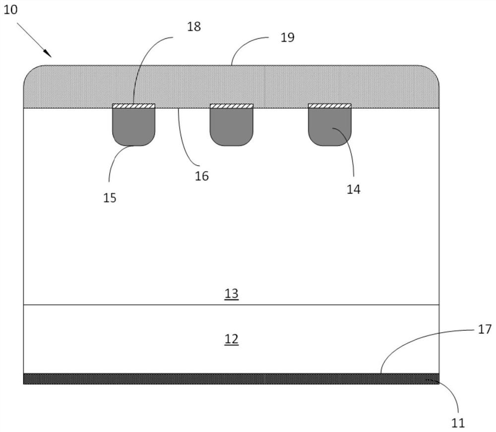
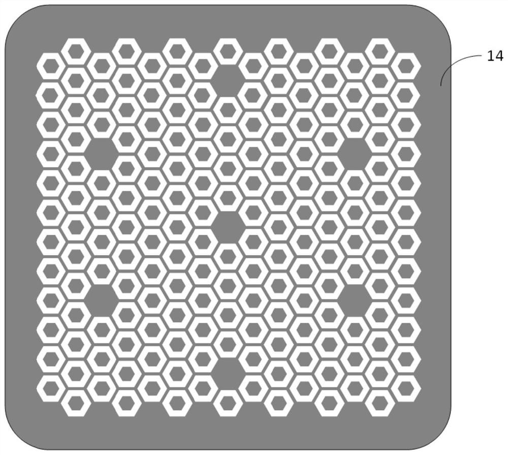
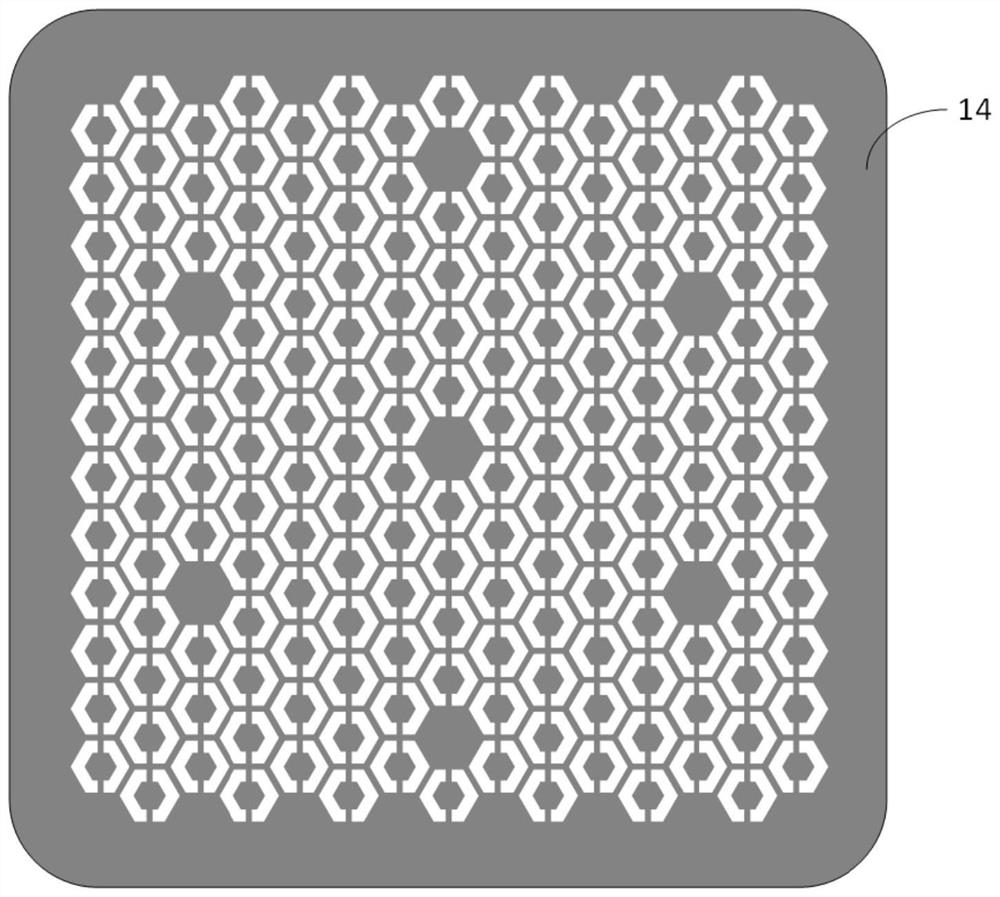
Composite PiN Schottky diode with plasma diffusion layer
A plasma and diffusion layer technology, applied in semiconductor devices, electrical components, circuits, etc., can solve the problems of device reliability reduction, performance degradation, failure, etc.
- Summary
- Abstract
- Description
- Claims
- Application Information
AI Technical Summary
Problems solved by technology
Method used
Image
Examples
Embodiment Construction
[0053] In order to explain the overall concept of the present application more clearly, the following detailed description will be given by way of examples in combination with the accompanying drawings.
[0054] The material of the semiconductor plays a decisive role in the performance of the semiconductor. The band gap of the silicon carbide semiconductor material is about three times that of the silicon material, and it has a higher critical breakdown electric field strength, a higher thermal conductivity, and a lower cost. Significant carrier concentration and higher saturation drift velocity make SiC an ideal material for high-voltage, high-temperature, high-power devices. For power diodes based on silicon carbide semiconductor materials, there are two technical routes for commercial devices, namely the junction barrier Schottky diode structure and the composite PiN Schottky diode structure.
[0055] Junction barrier Schottky diodes alternately arrange narrow P+ regions in...
PUM
| Property | Measurement | Unit |
|---|---|---|
| angle | aaaaa | aaaaa |
Abstract
Description
Claims
Application Information


