Semiconductor device

A semiconductor and device technology, applied in the field of semiconductor devices, can solve problems such as fragile, uneven heat dissipation, high heat, etc., and achieve the effects of improving distribution, improving anti-surge current capability, and improving overall performance and reliability

Pending Publication Date: 2020-11-10
ALPHA POWER SOLUTIONS LTD
View PDF0 Cites 0 Cited by
  • Summary
  • Abstract
  • Description
  • Claims
  • Application Information

AI Technical Summary

Problems solved by technology

Uneven heat dissipation can easily cause the device to generate excessive heat in some areas, making it very fragile and easily damaged, becoming one of the bottlenecks that limit the reliability of the device

Method used


Image

  • Semiconductor device
  • Semiconductor device
  • Semiconductor device

Examples


Embodiment Construction

[0031] Several exemplary embodiments of the present invention will be described below with reference to the associated drawings.

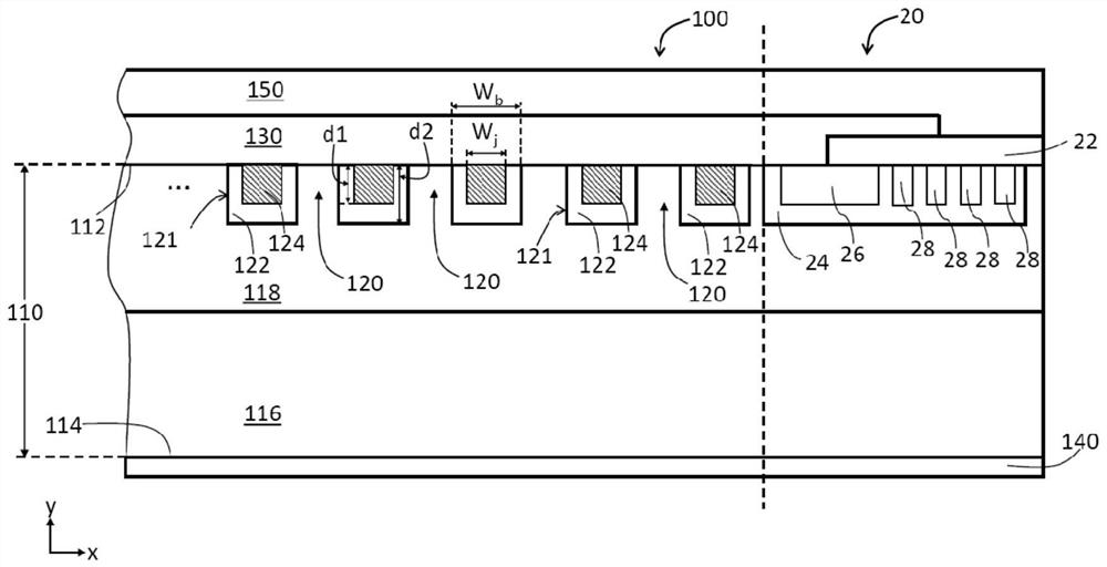
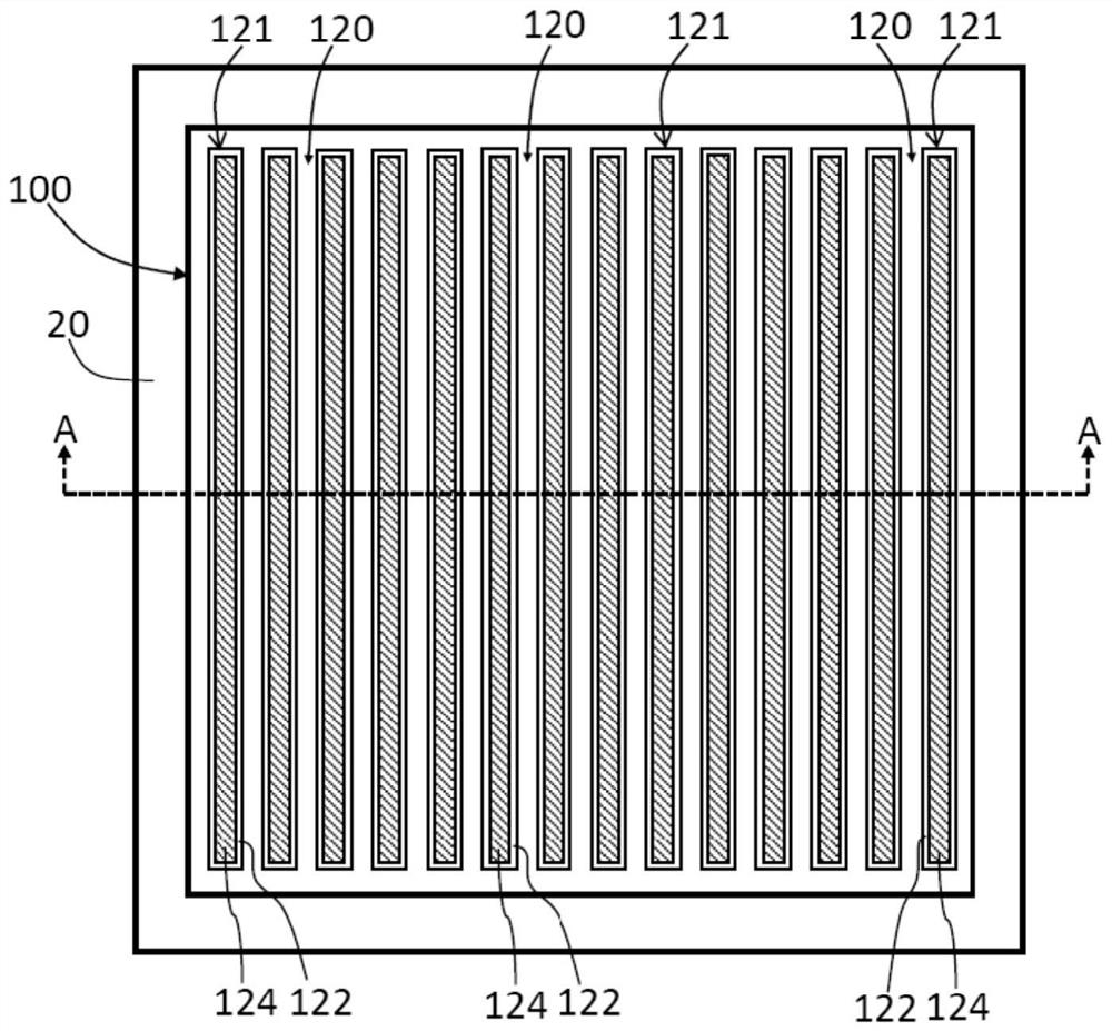
[0032] As used herein, the term "device region" refers to a region for carrying at least most of the current flowing in a semiconductor device and performing core functions of the semiconductor device under forward bias.

[0033] As used herein, the term "termination region" refers to a region in a semiconductor device at an end or edge of the device for providing protection to the device region.

[0034] As used herein, the term "Schottky region" refers to the region within the device region, located in the drift layer, below the Schottky junction formed by the contact between the drift layer and the metal electrode.

[0035] As used herein, the term "diode region" refers to a region in the drift layer of the device region having a conductivity type opposite to that of the drift layer.

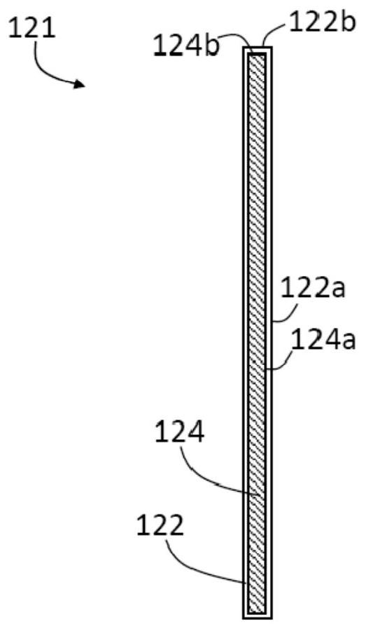
[0036] As used herein, the term "stripe" means that in a pl...


PUM

PropertyMeasurementUnit
thicknessaaaaaaaaaa

Abstract

The invention discloses a semiconductor device. The semiconductor device includes a device region and a terminal region surrounding the device region, and the device region includes a plurality of Schottky regions having a first conductivity type and a plurality of diode regions having a second conductivity type, and includes a central region and an edge region. The plurality of diode regions include a first plurality of diode regions and a second plurality of diode regions, the first plurality of diode regions are disposed in the central region, and the second plurality of diode regions are disposed in the edge region. The average impurity concentration of impurities of the second conductivity type in the first plurality of diode regions is higher than the average impurity concentration of impurities of the second conductivity type in the second plurality of diode regions. According to the semiconductor device provided by the invention, the current distribution in the device can be improved, the surge resistance of the device is improved, and the device has better electrical properties.

Description

technical field [0001] The present invention relates to the field of semiconductors, and more specifically, to semiconductor devices. Background technique [0002] Compared with silicon semiconductor devices, silicon carbide semiconductor devices can operate at higher temperatures and electric fields, so they have broad application prospects and market appeal. Various applications also require silicon carbide semiconductor devices to have high reliability, such as the ability to withstand surge currents. For example, junction barrier Schottky devices have been designed. This structure combines the advantages of the Schottky diode and the bipolar diode, and can greatly improve the anti-surge current capability of the Schottky device. [0003] However, the performance of junction barrier Schottky devices is highly dependent on layout design. When the current is relatively large, heat will be generated inside the device, which will increase the temperature of the device. Un...

Claims


Application Information

Patent Timeline
Patent Type & Authority Applications(China)
IPC IPC(8): H01L27/02H01L29/06
CPCH01L27/0255H01L29/0634
Inventor 陈伟钿张永杰周永昌王传道
Owner ALPHA POWER SOLUTIONS LTD
Why Eureka
Try Eureka