
Grid control diode with high surge current resistance

A gate-controlled diode and surge current technology, which is applied in the field of gate-controlled diodes, can solve the problems of reducing the reliability of the gate oxide layer of the gate-controlled diode, the thick drift region of the gate-controlled diode, and the inability to contribute to the surge current, etc., to improve The overall anti-surge capability, reducing the conduction voltage drop, and reducing the effect of recombination

Active Publication Date: 2022-05-27
NOVUS SEMICON CO LTD
View PDF10 Cites 0 Cited by
  • Summary
  • Abstract
  • Description
  • Claims
  • Application Information

AI Technical Summary

Problems solved by technology

[0006] However, with the improvement of the withstand voltage of the device, the thickness of the drift region of the gate-controlled diode becomes thicker and thicker, which leads to the fact that when we continue to use the traditional parasitic PIN diode for anti-surge current, the power consumption caused by the same surge current will decrease. With the increase of the thickness of the drift region, there is an exponential growth trend
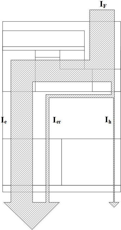
This is because the increase in the thickness of the drift region increases the diffusion length of the parasitic PIN diode minority carriers (holes) in the drift region, which will cause most of the minority carriers to be recombined in the drift region, so that they cannot contribute to the Inrush current
The electronic current formed by the recombination of minority carriers will be carried by the MOS channel, which reduces the reliability of the gate oxide layer of the gate-controlled diode.

Method used


Image

  • Grid control diode with high surge current resistance
  • Grid control diode with high surge current resistance
  • Grid control diode with high surge current resistance

Examples


Embodiment Construction

[0029] The principles and features of the present invention will be described below with reference to the accompanying drawings. The examples are only used to explain the present invention, but not to limit the scope of the present invention.

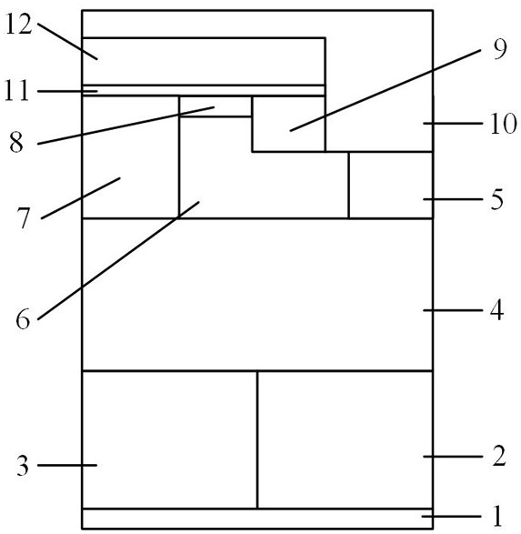
[0030] This embodiment provides a gated diode with high anti-surge current capability. The cell structure is as follows: figure 1 As shown, it includes backside ohmic contact alloy 1, N-type heavily doped substrate 3, P-type heavily doped substrate 2, N-type base region 4, P-type heavily doped emitter region 5, and P-type doped well region 6 , N-type doped JFET region 7, N-type heavily doped source region 9, N-type lightly doped channel 8, front metal 10, gate oxide layer 11 and polysilicon 12;

[0031] The N-type heavily doped substrate 3 is located at the upper left of the backside ohmic contact alloy 1; the P-type heavily doped substrate 2 is located at the upper right of the backside ohmic contact alloy 1; the N-type base region 4 ...


PUM


Abstract

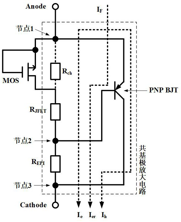
The invention relates to a grid-controlled diode with high surge current resistance, and belongs to the technical field of power semiconductor devices. According to the gate-controlled diode with the high surge current resistance, one-way current conduction is carried out by adopting a channel of an MOS (Metal Oxide Semiconductor). In order to reduce the forward conduction voltage drop of the diode, an accumulation channel is adopted to replace a conventional inversion channel. Besides, in order to improve the anti-surge capability of the device, PNP triodes which are connected in parallel are integrated for the grid-control diode, the addition of the triodes enables the base region of the triode to be conductively modulated when surge current arrives, the bulk resistance of the base region of the triode is reduced, and furthermore, the collector junction of the triode is reversely biased, so that the anti-surge capability of the device is improved. And the current entering the base region from the emitter region is further amplified.

Description

technical field [0001] The invention belongs to the technical field of power semiconductor devices, and in particular relates to a gate-controlled diode with high anti-surge current capability. Background technique [0002] Traditional power diodes are mainly divided into two categories: Schottky diodes and PIN diodes. [0003] Schottky diodes have become mainstream low-voltage devices (≤150V) thanks to their low manufacturing cost and low forward voltage drop, but due to the physical properties of the Schottky barrier itself (such as the electric field-induced barrier lowering effect) ) makes a significant increase in the leakage current of the Schottky in the high voltage and high temperature environment. Now, this makes the Schottky diode unable to be used in higher voltage scenarios. [0004] The barrier of PIN diodes is more stable than Schottky diodes, which makes them the first choice for high-temperature and high-voltage applications, but PIN diodes are bipolar devi...

Claims


Application Information

Patent Timeline
Patent Type & Authority Applications(China)
IPC IPC(8): H01L29/06H01L29/739
CPCH01L29/0603H01L29/0684H01L29/7391Y02P70/50
Inventor 顾航高巍戴茂州
Owner NOVUS SEMICON CO LTD
Learn More