Silicon carbide MPS diode with high surge current

A technology of inrush current and silicon carbide, which is applied in the field of diodes, can solve problems such as diode failure and large PN junction conduction voltage, and achieve the effects of reducing on-resistance, reducing chip temperature, and improving anti-surge current capability

Pending Publication Date: 2022-04-01
安徽长飞先进半导体有限公司
View PDF0 Cites 0 Cited by
  • Summary
  • Abstract
  • Description
  • Claims
  • Application Information

AI Technical Summary

Problems solved by technology

In order to ensure that the working current under normal operation meets the requirements, usually the PN junction area accounts for a small proportion of the total chip area. Due to the small proportion of the PN junction area to the total chip area, the PN junction conduction voltage is large, and the PN junction is under the impact of surge current. The junction is not conducting, causing the diode to fail prematurely

Method used


Image

  • Silicon carbide MPS diode with high surge current
  • Silicon carbide MPS diode with high surge current
  • Silicon carbide MPS diode with high surge current

Examples


Embodiment Construction

[0022] Referring to the accompanying drawings, through the description of the embodiments, the specific embodiments of the present invention include the shape, structure, mutual position and connection relationship of each part, the function and working principle of each part, and the manufacturing process of the various components involved. And the method of operation and use, etc., are described in further detail to help those skilled in the art have a more complete, accurate and in-depth understanding of the inventive concepts and technical solutions of the present invention.

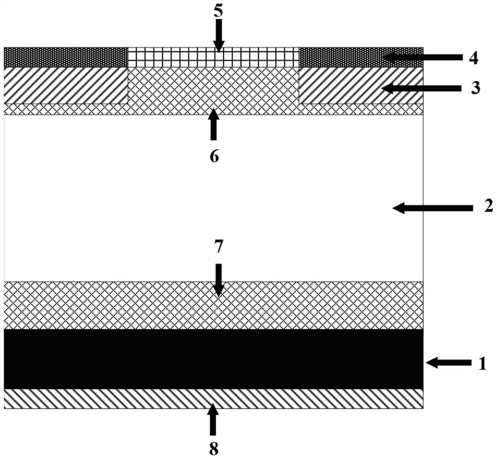
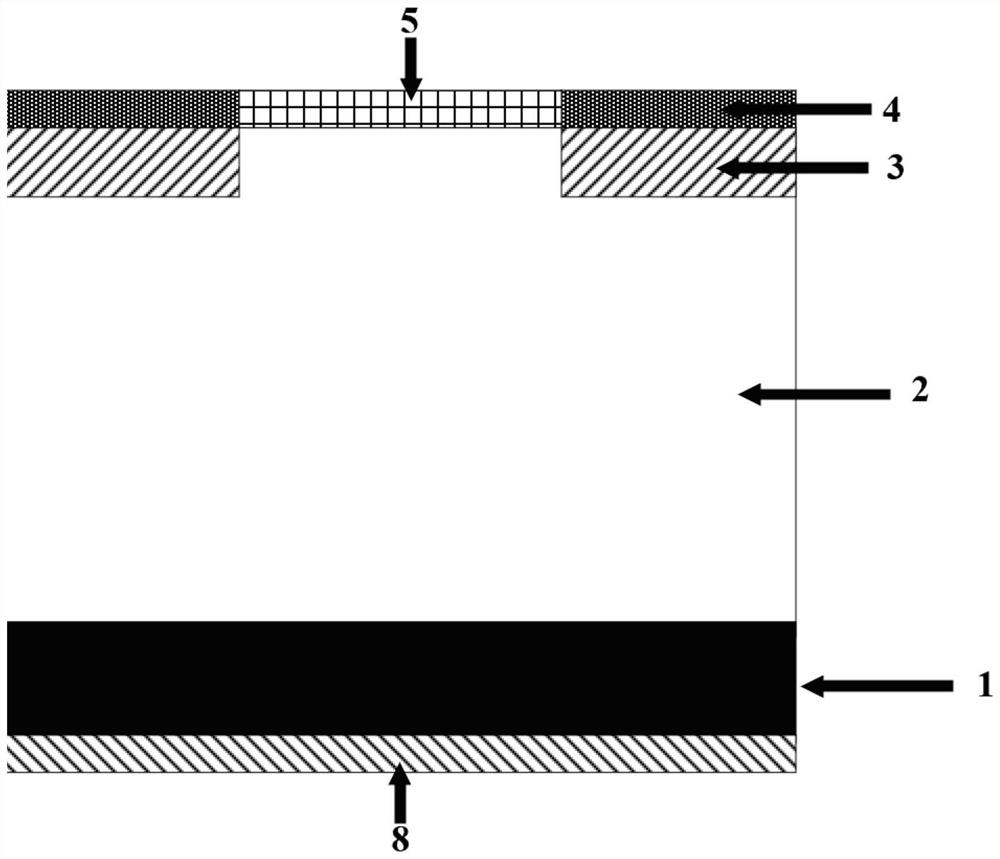
[0023] Such as figure 1 As shown, it is a schematic diagram of the silicon carbide MPS diode layer structure with high surge current in the present invention, including ohmic contact electrode 4, silicon carbide N+ substrate 1, silicon carbide N- epitaxial layer 2, Schottky contact electrode 5, multiple P+ injection region 3, first bipolar transport layer 6, second bipolar transport layer 7, cathode ...


PUM


Abstract

The invention discloses a silicon carbide MPS diode with high surge current, which is formed by sequentially stacking a cathode ohmic contact electrode, a silicon carbide N + substrate and a silicon carbide N-epitaxial layer, a plurality of P + injection regions are arranged on the silicon carbide N-epitaxial layer at intervals, ohmic contact electrodes are arranged on the P + injection regions, and the ohmic contact electrodes are arranged on the silicon carbide N + substrate. Gaps between the ohmic contact electrodes are filled with Schottky contact electrodes, and bipolar transmission layers are arranged on the two sides of the silicon carbide N-epitaxial layer. According to the MPS diode, due to the existence of the variously doped bipolar transmission layer, the PN junction conduction voltage of the MPS diode is reduced, the diode can enter a bipolar working state in advance under a lower current, a conductivity modulation effect is generated, the conduction resistance of the diode is reduced, the chip temperature of the diode under a large current is reduced, and the performance of the MPS diode is improved. Therefore, the surge current resistance of the diode is improved, and the reverse breakdown voltage of the MPS diode can also be improved.

Description

technical field [0001] The invention relates to the technical field of diodes. Background technique [0002] Silicon carbide (SiC), a wide bandgap semiconductor material, is an ideal material for preparing high-voltage power electronic devices. Compared with Si materials, SiC materials have a higher breakdown electric field strength (4×10 6 V / cm), high carrier saturation drift velocity (2×10 7 cm / s), high thermal conductivity, and good thermal stability, so it is especially suitable for high-power, high-pressure, and high-temperature application scenarios. SiC Junction Barrier Schottky Diodes (JBS), as the earliest commercialized product in SiC power devices, now occupy the largest number of market shares. Through the potential barrier formed by the contact between SiC semiconductor and metal, the rectification effect of conducting in one direction and blocking in one direction is realized. The advantages of JBS diodes in power systems are the advantages of low on-resista...

Claims


Application Information

Patent Timeline
Patent Type & Authority Applications(China)
IPC IPC(8): H01L29/06H01L29/868H01L29/872
Inventor 罗茂久邢婷婷钮应喜袁松彭强乔庆楠
Owner 安徽长飞先进半导体有限公司
Why Eureka
Try Eureka